


 Marcy's Musings: The Growing Industry
 It’s Only Common Sense: Here’s What To Do After IPC APEX EXPO 2024
 Dan’s Biz Bookshelf: Seeing the How
Laser Patterning & Metallization to Reduce Process Steps for PCB Manufacturing
August 29, 2017 | Joel Schrauben, Cameron Tribe, Christopher Ryder and Jan Kleinert, ELECTRO SCIENTIFIC INDUSTRIESEstimated reading time: 1 minute
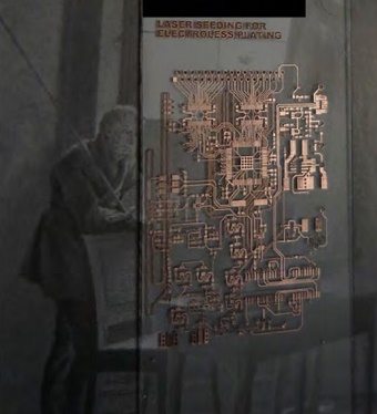
Abstract
Glass offers a number of advantages as a dielectric material, such as a low coefficient of thermal expansion (CTE), high dimensional stability, high thermal conductivity and suitable dielectric constant. These properties make glass an ideal candidate for, among other things, package substrate and high-frequency PCB applications. We report here a novel process for the production of printed circuit boards and integrated circuit packaging using glass as both a dielectric medium and a platform for wiring simultaneously.
An ultrafast laser is used to etch away the desired pattern (pads, wires and vias) in the glass, and copper plating is “seeded” through the laser-based deposition of copper droplets. The seeded area is then plated using electroless plating followed by electroplating. Demonstrations of fine pitch wires, variable diameter through holes and blind vias, and a multilayer stack are shown. The deposits have a resistivity less than a factor of 1.5x that of bulk copper for 5-10 mm wires. Plated lines in borosilicate glass of 7-10 μm width and 5-20 μm depth and line spacing down to ~10 μm are demonstrated, as well as vias with a top diameter approaching 100 μm for 150 μm glass and 40 μm for 50 μm glass.
The process presents the potential for significant material savings in terms of base materials, process chemicals, and waste disposal/recycling costs (glass is on the order of 100-fold less expensive than some current high-frequency dielectrics, and wet processes account for a large part of standard PCB/substrate manufacturing). Additionally, the processes are amenable toward other dielectric materials such as FR-4, polyimide and PTFE-based materials.
Introduction
Increased demand for high data transmission rates is driving the development of smaller PCB features. Electrical circuits are reaching the physical limitations of traditional PCB dielectric materials under which electromagnetic compatibility can be controlled.
To read the full version of this article which appeared in the August 2017 issue of The PCB Magazine, click here.
Share on:


Suggested Items
Insulectro’s 'Storekeepers' Extend Their Welcome to Technology Village at IPC APEX EXPO
04/03/2024 | InsulectroInsulectro, the largest distributor of materials for use in the manufacture of PCBs and printed electronics, welcomes attendees to its TECHNOLOGY VILLAGE during this year’s IPC APEX EXPO at the Anaheim Convention Center, April 9-11, 2024.
ENNOVI Introduces a New Flexible Circuit Production Process for Low Voltage Connectivity in EV Battery Cell Contacting Systems
04/03/2024 | PRNewswireENNOVI, a mobility electrification solutions partner, introduces a more advanced and sustainable way of producing flexible circuits for low voltage signals in electric vehicle (EV) battery cell contacting systems.
Heavy Copper PCBs: Bridging the Gap Between Design and Fabrication, Part 1
04/01/2024 | Yash Sutariya, Saturn Electronics ServicesThey call me Sparky. This is due to my talent for getting shocked by a variety of voltages and because I cannot seem to keep my hands out of power control cabinets. While I do not have the time to throw the knife switch to the off position, that doesn’t stop me from sticking screwdrivers into the fuse boxes. In all honesty, I’m lucky to be alive. Fortunately, I also have a talent for building high-voltage heavy copper circuit boards. Since this is where I spend most of my time, I can guide you through some potential design for manufacturability (DFM) hazards you may encounter with heavy copper design.
Trouble in Your Tank: Supporting IC Substrates and Advanced Packaging, Part 5
03/19/2024 | Michael Carano -- Column: Trouble in Your TankDirect metallization systems based on conductive graphite or carbon dispersion are quickly gaining acceptance worldwide. Indeed, the environmental and productivity gains one can achieve with these processes are outstanding. In today’s highly competitive and litigious environment, direct metallization reduces costs associated with compliance, waste treatment, and legal issues related to chemical exposure. What makes these processes leaders in the direct metallization space?
AT&S Shines with Purest Copper on World Recycling Day
03/18/2024 | AT&SThe Styrian microelectronics specialist AT&S is taking World Recycling Day as an opportunity to review the progress that has been made in recent months at its sites around the world in terms of the efficient use of resources: