


 Marcy's Musings: The Growing Industry
 It’s Only Common Sense: Here’s What To Do After IPC APEX EXPO 2024
 Dan’s Biz Bookshelf: Seeing the How
Scientists Fine-Tune Organic Thin Films With an Eye Toward Biomedical Devices
October 2, 2017 | OSAEstimated reading time: 5 minutes
Using DNA from salmon, researchers in South Korea hope to make better biomedical and other photonic devices based on organic thin films. Often used in cancer treatments and health monitoring, thin films have all the capabilities of silicon-based devices with the possible added advantage of being more compatible with living tissue.
A thin film is just what it sounds like, a layer of material only nanometers or micrometers thick that can be used to channel light. If the film is a dielectric—that is, an insulator such as glass—it can be used without worrying that it might conduct electricity.
“DNA is the most abundant organic material, and it is a transparent dielectric, comparable to silica,” said Kyunghwan “Ken” Oh, of the Photonic Device Physics Laboratory at Yonsei University, Seoul, South Korea. In the journal Optical Materials Express, from The Optical Society (OSA), Oh and his colleagues lay out their method for fabricating the thin films in a way that gives them fine control over the material’s optical and thermal properties.
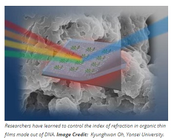
Researchers have learned to control the index of refraction in organic thin films made out of DNA. Image Credit: Kyunghwan Oh, Yonsei University.
As the basis for the silica glass that makes up optical fibers, silicon has long been a dominant material in inorganic photonic devices because it’s readily available and easy to work with from the materials perspective. Oh argues that DNA can play the same role in organic photonic devices because it can be found throughout the living world. It could, for instance, be used to make waveguides similar to silica fibers to carry light within the body. Organic devices should also be easy to manufacture, more flexible than silicon and environmentally friendly.
‘A sharper arrow’
One key property of materials used in photonic devices is the refractive index, which determines how light is directed. An optical fiber requires a core with one index, wrapped in a cladding with a different enough index so that when light hits the interface between core and cladding, it is forced back into the core instead of leaking away. Makers of optical fiber not only need material with two different refractive indexes, they need to control the magnitude of that difference to get the desired effects.
In fine-tuning a method for using DNA to create thin films that could be used in photonic devices, Oh’s team was able to get a range of refractive indexes four times greater than that available in silicon. With a greater index difference between core and cladding, they can make much thinner optical fibers, as low as 3 microns in diameter, compared to a minimum of 10 in silicon. This allows for a smaller spot size for the light coming out of the fiber, which could be useful in applications that must carefully target light. “If you have a small target, you should have a sharper arrow,” said Oh.
Potential applications could include photodynamic therapy, where a cancer patient is given a drug or other substance that binds to cells in a tumor and light activates the drug and destroys the cancer cells, leaving healthy tissue untouched. The films may also be useful in optogenetics, in which light is used to control the activity of specific brain cells, or to make sensors to measure the pressure or oxygen content of blood pressure that could be worn for a long time without causing irritation because they are organic.
Grappling with inconsistent results
To make a thin film, which can be used as the basis for photonic devices, researchers have to dissolve DNA in water, and then dissolve that mixture into an organic solvent. The liquid is placed on a surface, which spins so the material spreads evenly. The solvent then evaporates to leave the film behind. Because DNA doesn’t readily dissolve, researchers first mix it with a solution of water and cetyltrimethylammonium (CTMA), a soap-like surfactant. The mixture produces a precipitate, which can then be dissolved into the solvent and spin-coated.
While researchers have used this procedure for several years, their results have been inconsistent. “We noticed that, depending on the papers, the refractive index and material properties varied in a wide range, so we were very curious about it,” said Oh. “And we found out the fabrication process was a little bit different from research group to research group.”
Controlling the process
Three graduate students in Oh’s lab—Woohyun Jung, Hwiseok Jun and Seongjin Hong—found that by controlling the amount of water and CTMA in their mixture, they could fine-tune the refractive index of the thin film. Testing revealed different mixtures, depending on whether they added droplets of water and DNA into the CTMA solution, or water and CTMA into the DNA bath. Oh describes the strand of DNA as a rope, with sites along it to which the CTMA can bind. “If you drop this rope into a CTMA bath, there are tons of CTMA available, so you can soak the rope with the CTMA,” said Oh. On the other hand, if you drop CTMA onto a large batch of DNA, the “rope” may not get completely wet; that is, there are areas of DNA without CTMA attached.
The more water the mixture contained, the less CTMA there was, and vice versa. By carefully controlling the amount of both, the team could achieve the desired index of refraction. The same approach provided control over the thermal properties of the film, allowing the researchers to control how much the refractive index changed when the film was heated or cooled. That could allow the film to be used as a temperature sensor, as changes in the light passing through it would be linked to changes in temperature.
Oh’s lab is also exploring other methods to control the optical properties of DNA. His hope is to develop a set of fundamental principles and processes that will allow manufacturers to build a wide range of optical devices, including a new generation of wearable sensors.
About Optical Materials Express
Optical Materials Express (OMEx) is an open-access journal focusing on the synthesis, processing and characterization of materials for applications in optics and photonics. OMEx, which launched in April 2011, primarily emphasizes advances in novel optical materials, their properties, modeling, synthesis and fabrication techniques; how such materials contribute to novel optical behavior; and how they enable new or improved optical devices. It is published by The Optical Society and edited by Alexandra Boltasseva.
About The Optical Society
Founded in 1916, The Optical Society (OSA) is the leading professional organization for scientists, engineers, students and business leaders who fuel discoveries, shape real-life applications and accelerate achievements in the science of light. Through world-renowned publications, meetings and membership initiatives, OSA provides quality research, inspired interactions and dedicated resources for its extensive global network of optics and photonics experts.
Share on:


Suggested Items
Groundbreaking Ceremony Marks the Beginning of a New Era for Newccess Industrial; The Construction of the MINGXIN Building
04/12/2024 | Newccess IndustrialOn a clear and sunny day in March, the groundbreaking ceremony for the MINGXIN Building took place in Shenzhen, China. This moment marked the official commencement of construction for a project that will reshape the semiconductor materials industry.
The Need for a Holistic Global Sustainability Standard
04/10/2024 | Michael Ford, Aegis SoftwareNo one can deny that the resources of our fragile planet are finite. The environment seems like a third party, subject to constant degradation. We’re acutely aware of the effects of pollution on our climate, and despite our “throw-away” culture, recycling and recovery of materials has remained relatively expensive, even as we use more energy just to survive.
iNEMI Publishes Four Roadmap Topics
04/04/2024 | iNEMIThe International Electronics Manufacturing Initiative (iNEMI) announces the availability of the first roadmap topics in the new iNEMI Roadmap format. Printed circuit boards, sustainable electronics, smart manufacturing, and mmWave materials and test are now available online.
Insulectro’s 'Storekeepers' Extend Their Welcome to Technology Village at IPC APEX EXPO
04/03/2024 | InsulectroInsulectro, the largest distributor of materials for use in the manufacture of PCBs and printed electronics, welcomes attendees to its TECHNOLOGY VILLAGE during this year’s IPC APEX EXPO at the Anaheim Convention Center, April 9-11, 2024.
Checking In With ICAPE Group
04/03/2024 | Nolan Johnson, I-Connect007ICAPE Group’s field application engineer Erik Pederson drills down on sustainability, supply chain resiliency, and what value engineering really looks like in this exclusive interview. Founded in 1999, European-based ICAPE Group provides 21 million printed circuit boards and over six million technical parts to manufacturers every month. With 30 PCB manufacturing partners globally and 50 partners providing a wide array of technical parts, ICAPE Group has operations in China, Taiwan, Thailand, South Korea, Vietnam, South Africa, Europe, Mexico, and the United States. The company also focuses on the value proposition for its customers.