


 Marcy's Musings: The Growing Industry
 It’s Only Common Sense: Here’s What To Do After IPC APEX EXPO 2024
 Dan’s Biz Bookshelf: Seeing the How
AT&S Demonstrates Efficiency and Robustness of Embedded Power Technology
April 5, 2019 | AT&SEstimated reading time: 3 minutes
To improve the efficiency in modern cars on the way to electromobility and in challenging industrial power conversion applications the power density has to be increased without limitations on performance and reliability. Based on the AT&S ECP (Embedded Components Packaging) technology, active and passive components have been integrated into PCBs for low-power designs and are used in volume production meeting high-quality requirements. Against this background, the implementation of power semiconductors like MOSFETs or diodes directly into the PCB is a very promising approach to fulfill the increasing needs of electromobility and industrial applications. AT&S successfully used the expertise with its ECP technology for the implementation of efficient power packages and modules. Compared to SMT-based technology a space reduction for the power module of 50% could be realized. In addition, very good results in terms of switching behavior, heat removal and power cycling robustness were achieved.
The EmPower Project
The EUREKA CATRENE “EmPower” project, with the goal to develop a technology for embedded power components for electrical vehicle applications, was running from May 2013 to February 2017. The project was coordinated by AT&S and included ST Microelectronics, Atotech, ILFA, Continental, TU Wien and TU Berlin as further members.
Interconnections between the power devices and wire bonds on direct copper bonded (DCB) substrates are a primary source of parasitic inductances in today’s power packages, leading to significant switching losses, limited lifetime and reliability issues due to the high-power loss density. In contrast, the EmPower embedding concept contains copper interconnections with large cross sections between the power devices and the chip pads by short copper-filled via and large copper cross section. This technology allows the placement of the necessary copper connections and pads on both sides of the package in an arbitrary manner, thus satisfying the needs for both, high electrical and high thermal conductivities. On the other hand, the concept sees the power semiconductors being coated on both sides with copper and embedded in a printed circuit board construction using a galvanic interconnection process. Lastly, making the shortest possible electrical connections between the power semiconductors is minimizing the parasitic inductances and significantly improving the switching performance.
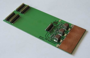
At the heart of the EmPower implementation are so-called power cores as function blocks for power modules. The innovation in terms of the new power concept entails the embedding of power devices such as MOSFETs and diodes as chips with significantly reduced thicknesses in comparison to SMT devices. Cost-effective and effective thermal management is realized by embedding the power semiconductors in a module enabling double sided cooling. This technology allows power semiconductors to be embedded in such a way that the rear of the power module provides a complete copper surface for the connection and allows chips of up to 10 mm x 10 mm to be embedded. The contacting of the pads on the upper side of the components is done by means of micro-via and full area interconnection on the lower side of the devices.
Demonstrators Show High Robustness and Electrical Performance
In order to evaluate the scalability and performance of the new power embedding technology, several demonstrators in the range from 50W to 50kW were developed. The corresponding demonstrators have been realized as a power package (50W, 100V, 20A), a power module (500W, 12-48V, 20A) for a pedelec application and a 50kW power inverter (250V−450V, 200A) for hybrid/electric vehicle applications.
Thermal behavior and electrical performance were investigated successfully with various tests with the 50W and 500W demonstrators in comparison to a standard SMT power package solution as benchmark.
Active power cycling is another important test for power electronic components and modules. Tests with the 500W demonstrator passed more than 300.000 cycles. Other projects with various temperature conditions and stress types show the successful pass of 600.000 cycles and more.
To summarize the outcome of the Embedded Power Project, the concept has shown high potentials according miniaturization, switching performance and thermal management. Reliability according AEC-Q101 have been shown with different tests like power cycling. The technology promises high robustness for power embedding application.
Share on:


Suggested Items
Insulectro’s 'Storekeepers' Extend Their Welcome to Technology Village at IPC APEX EXPO
04/03/2024 | InsulectroInsulectro, the largest distributor of materials for use in the manufacture of PCBs and printed electronics, welcomes attendees to its TECHNOLOGY VILLAGE during this year’s IPC APEX EXPO at the Anaheim Convention Center, April 9-11, 2024.
ENNOVI Introduces a New Flexible Circuit Production Process for Low Voltage Connectivity in EV Battery Cell Contacting Systems
04/03/2024 | PRNewswireENNOVI, a mobility electrification solutions partner, introduces a more advanced and sustainable way of producing flexible circuits for low voltage signals in electric vehicle (EV) battery cell contacting systems.
Heavy Copper PCBs: Bridging the Gap Between Design and Fabrication, Part 1
04/01/2024 | Yash Sutariya, Saturn Electronics ServicesThey call me Sparky. This is due to my talent for getting shocked by a variety of voltages and because I cannot seem to keep my hands out of power control cabinets. While I do not have the time to throw the knife switch to the off position, that doesn’t stop me from sticking screwdrivers into the fuse boxes. In all honesty, I’m lucky to be alive. Fortunately, I also have a talent for building high-voltage heavy copper circuit boards. Since this is where I spend most of my time, I can guide you through some potential design for manufacturability (DFM) hazards you may encounter with heavy copper design.
Trouble in Your Tank: Supporting IC Substrates and Advanced Packaging, Part 5
03/19/2024 | Michael Carano -- Column: Trouble in Your TankDirect metallization systems based on conductive graphite or carbon dispersion are quickly gaining acceptance worldwide. Indeed, the environmental and productivity gains one can achieve with these processes are outstanding. In today’s highly competitive and litigious environment, direct metallization reduces costs associated with compliance, waste treatment, and legal issues related to chemical exposure. What makes these processes leaders in the direct metallization space?
AT&S Shines with Purest Copper on World Recycling Day
03/18/2024 | AT&SThe Styrian microelectronics specialist AT&S is taking World Recycling Day as an opportunity to review the progress that has been made in recent months at its sites around the world in terms of the efficient use of resources: