


 It’s Only Common Sense: OCCAM—the Time Is Now
 Marcy's Musings: The Growing Industry
 Dan’s Biz Bookshelf: Seeing the How
Decoupled Graphene Thanks to Potassium Bromide
April 29, 2019 | University of BaselEstimated reading time: 2 minutes
The use of potassium bromide in the production of graphene on a copper surface can lead to better results. When potassium bromide molecules arrange themselves between graphene and copper, it results in electronic decoupling. This alters the electrical properties of the graphene produced, bringing them closer to pure graphene, as reported by physicists from the universities of Basel, Modena and Munich in the journal ACS Nano.
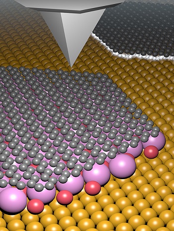
Image Caption: Potassium bromide molecules (pink) arrange themselves between the copper substrate (yellow) and the graphene layer (gray). This brings about electrical decoupling, as demonstrated by scanning probe microscopy studies.
Graphene consists of a layer of carbon atoms just one atom in thickness in a honeycomb pattern and is the subject of intensive worldwide research. Thanks to its high level of flexibility, combined with excellent stability and electrical conductivity, graphene has numerous promising applications—particularly in electronic components.
Molecules for Decoupling
Graphene is often produced via a chemical reaction on metallic surfaces in a process known as chemical vapor deposition. The graphene layer and the underlying metal are then electrically coupled, which diminishes some of the special electrical properties of graphene. For use in electronics, the graphene has to be transferred onto insulating substrates in a multistep process, during which there is a risk of damage and contamination.
In order to obtain defect-free, pure graphene, it is therefore preferable to decouple the graphene electrically from the metallic substrate and to develop a method that allows easier transfer without damage. The group led by Professor Ernst Meyer from the Department of Physics and the Swiss Nanoscience Institute (SNI) of the University of Basel is investigating ways of incorporating molecules between the graphene layer and the substrate after the chemical deposition process, which leads to this type of decoupling.
Altering Electrical Properties
In a study carried out by SNI doctoral student Mathias Schulzendorf, scientists have shown that potassium bromide is ideally suited to this. Potassium bromide is a soluble hydrogen bromide salt. Unlike the chemically similar compound sodium chloride, potassium bromide molecules arrange themselves between the graphene layer and the copper substrate. This was demonstrated by researchers in a variety of scanning probe microscopy studies.
Calculations performed by colleagues at the University of Modena and Reggio Emilia (Italy) explain this phenomenon: It is more energetically advantageous for the system if potassium bromide molecules arrange themselves between the graphene and copper than if they are deposited on the graphene—as happens with sodium chloride.
The researchers have shown that the intermediate layer of potassium bromide alters the electrical properties of graphene—until they correspond to those expected for free graphene. “Our work has demonstrated that the graphene and the underlying metal can be decoupled using potassium bromide, bringing us a key step closer to producing clean and defect-free graphene,” says project supervisor Dr. Thilo Glatzel, who is a member of Meyer’s team.
Share on:


Suggested Items
Insulectro’s 'Storekeepers' Extend Their Welcome to Technology Village at IPC APEX EXPO
04/03/2024 | InsulectroInsulectro, the largest distributor of materials for use in the manufacture of PCBs and printed electronics, welcomes attendees to its TECHNOLOGY VILLAGE during this year’s IPC APEX EXPO at the Anaheim Convention Center, April 9-11, 2024.
ENNOVI Introduces a New Flexible Circuit Production Process for Low Voltage Connectivity in EV Battery Cell Contacting Systems
04/03/2024 | PRNewswireENNOVI, a mobility electrification solutions partner, introduces a more advanced and sustainable way of producing flexible circuits for low voltage signals in electric vehicle (EV) battery cell contacting systems.
Heavy Copper PCBs: Bridging the Gap Between Design and Fabrication, Part 1
04/01/2024 | Yash Sutariya, Saturn Electronics ServicesThey call me Sparky. This is due to my talent for getting shocked by a variety of voltages and because I cannot seem to keep my hands out of power control cabinets. While I do not have the time to throw the knife switch to the off position, that doesn’t stop me from sticking screwdrivers into the fuse boxes. In all honesty, I’m lucky to be alive. Fortunately, I also have a talent for building high-voltage heavy copper circuit boards. Since this is where I spend most of my time, I can guide you through some potential design for manufacturability (DFM) hazards you may encounter with heavy copper design.
Trouble in Your Tank: Supporting IC Substrates and Advanced Packaging, Part 5
03/19/2024 | Michael Carano -- Column: Trouble in Your TankDirect metallization systems based on conductive graphite or carbon dispersion are quickly gaining acceptance worldwide. Indeed, the environmental and productivity gains one can achieve with these processes are outstanding. In today’s highly competitive and litigious environment, direct metallization reduces costs associated with compliance, waste treatment, and legal issues related to chemical exposure. What makes these processes leaders in the direct metallization space?
AT&S Shines with Purest Copper on World Recycling Day
03/18/2024 | AT&SThe Styrian microelectronics specialist AT&S is taking World Recycling Day as an opportunity to review the progress that has been made in recent months at its sites around the world in terms of the efficient use of resources: