


 Marcy's Musings: The Growing Industry
 It’s Only Common Sense: Here’s What To Do After IPC APEX EXPO 2024
 Dan’s Biz Bookshelf: Seeing the How
Breakthrough Material Could Lead to Cheaper, More Widespread Solar Panels and Other Electronics
July 17, 2019 | The University of KansasEstimated reading time: 4 minutes
Imagine printing electronic devices using a simple inkjet printer — or even painting a solar panel onto the wall of a building.
Such technology would slash the cost of manufacturing electronic devices and enable new ways to integrate them into our everyday lives. Over the last two decades, a type of material called organic semiconductors, made out of molecules or polymers, has been developed for such purposes. But some properties of these materials pose a major hurdle that limits their widespread use.
“In these materials, an electron is usually bound to its counterpart, a missing electron known as ‘hole,’ and can’t move freely,” said Wai-Lun Chan, associate professor of physics & astronomy at the University of Kansas. “So-called ‘free electrons,’ which wander freely in the material and conduct electricity, are rare and can’t be generated readily by light absorption. This impedes the use of these organic materials in applications like solar panels because panels built with these materials often have poor performance.”
Because of this problem, Chan said “freeing the electrons” has been a focus in developing organic semiconductors for solar cells, light sensors and many other optoelectronic applications.
Now, two physics research groups at KU, led by Chan and Hui Zhao, professor of physics & astronomy, have effectively generated free electrons from organic semiconductors when combined with a single atomic layer of molybdenum disulfide (MoS2), a recently discovered two-dimensional (2D) semiconductor.
The introduced 2D layer allows the electrons to escape from “holes” and move freely. The findings have just been published in the Journal of American Chemical Society, a leading journal in chemistry and interfacing areas of science.
Over the last few years, many researchers have been investigating how free charges can be generated effectively from hybrid organic-2D interfaces.
“One of the prevailing assumptions is free electrons can be generated from the interface as long as electrons can be transferred from one material to another in a relatively short period of time — less than one-trillionth of a second,” Chan said. “However, my graduate students Tika Kafle and Bhupal Kattel and I have found the presence of the ultrafast electron transfer in itself is not sufficient to guarantee the generation of free electrons from the light absorption. That’s because the ‘holes’ can prevent the electrons from moving away from the interface. Whether the electron can be free from this binding force depends on the local energy landscape near the interface.”
Chan said the energy landscape of the electrons could be seen as a topographic map of a mountain.
“A hiker chooses his path based on the height contour map,” he said. “Similarly, the motion of the electron at the interface between the two materials is controlled by the electron energy landscape near the interface.”
Chan and Zhao’s findings will help develop general principles of how to design the “landscape” to free the electrons in such hybrid materials.
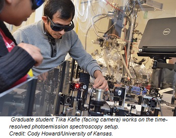
The discovery was made by combining two highly complementary experimental tools based on ultrafast lasers, time-resolved photoemission spectroscopy in Chan's lab and transient optical absorption in Zhao's lab. Both experimental setups are located in the basement of the Integrated Science Building.
In the time-resolved photoemission spectroscopy experiment, Kafle used an ultrashort laser pulse that only exists for 10-quadrillionths (10-14) of a second to trigger the motion of electrons. The advantage of using such a short pulse is the researcher knows precisely the starting time of the electron’s journey. Kafle then used another ultrashort laser pulse to hit the sample again at an accurately controlled time relative to the first pulse. This second pulse is energetic enough to kick out these electrons from the sample. By measuring the energy of these electrons (now in a vacuum) and using the principle of energy conservation, the researchers were able to figure out the energy of electrons before they were kicked out and thus reveal the journey of these electrons since they were hit by the first pulse. This technique resolved the energy of the excited electrons as it moves across the interface after the light absorption. Because only electrons near the front surface of the sample can be released by the second pulse, the position of the electron relative to the interface is also revealed with atomic precision.
In the transient optical absorption measurements, Peng Yao (a visiting student) and KU graduate Peymon Zereshki, both supervised by Zhao, also used a two-pulse technique, with the first pulse initiating the electron motion in the same way. However, in their measurements, the second pulse does the trick of monitoring electrons by detecting the fraction of the second pulse that is reflected from the sample, instead of kicking out the electrons.
“Because light can penetrate a longer distance, the measurement can probe electrons in the entire depth of the sample and therefore provide complementary information to the first techniques that are more ‘surface sensitive,’” Zhao said. “These detailed measurements enabled us to reconstruct the trajectory of the electron and determine conditions that enable the effective generation of free electrons.”
The collaborative work from the two research teams will provide a blueprint on how to design interfaces that can turn light into electrical current with high efficiency. Both teams are funded by the National Science Foundation through a CAREER Award (Chan) and a Condensed Matter Physics Award (Zhao).
Share on:


Suggested Items
Groundbreaking Ceremony Marks the Beginning of a New Era for Newccess Industrial; The Construction of the MINGXIN Building
04/12/2024 | Newccess IndustrialOn a clear and sunny day in March, the groundbreaking ceremony for the MINGXIN Building took place in Shenzhen, China. This moment marked the official commencement of construction for a project that will reshape the semiconductor materials industry.
The Need for a Holistic Global Sustainability Standard
04/10/2024 | Michael Ford, Aegis SoftwareNo one can deny that the resources of our fragile planet are finite. The environment seems like a third party, subject to constant degradation. We’re acutely aware of the effects of pollution on our climate, and despite our “throw-away” culture, recycling and recovery of materials has remained relatively expensive, even as we use more energy just to survive.
iNEMI Publishes Four Roadmap Topics
04/04/2024 | iNEMIThe International Electronics Manufacturing Initiative (iNEMI) announces the availability of the first roadmap topics in the new iNEMI Roadmap format. Printed circuit boards, sustainable electronics, smart manufacturing, and mmWave materials and test are now available online.
Insulectro’s 'Storekeepers' Extend Their Welcome to Technology Village at IPC APEX EXPO
04/03/2024 | InsulectroInsulectro, the largest distributor of materials for use in the manufacture of PCBs and printed electronics, welcomes attendees to its TECHNOLOGY VILLAGE during this year’s IPC APEX EXPO at the Anaheim Convention Center, April 9-11, 2024.
Checking In With ICAPE Group
04/03/2024 | Nolan Johnson, I-Connect007ICAPE Group’s field application engineer Erik Pederson drills down on sustainability, supply chain resiliency, and what value engineering really looks like in this exclusive interview. Founded in 1999, European-based ICAPE Group provides 21 million printed circuit boards and over six million technical parts to manufacturers every month. With 30 PCB manufacturing partners globally and 50 partners providing a wide array of technical parts, ICAPE Group has operations in China, Taiwan, Thailand, South Korea, Vietnam, South Africa, Europe, Mexico, and the United States. The company also focuses on the value proposition for its customers.