


 Marcy's Musings: The Growing Industry
 It’s Only Common Sense: Here’s What To Do After IPC APEX EXPO 2024
 Dan’s Biz Bookshelf: Seeing the How
DGIST Achieves the Highest Efficiency of Flexible CZTSSe Thin-Film Solar Cell
September 19, 2019 | DGISTEstimated reading time: 2 minutes
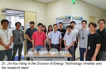
DGIST announced on Tuesday, September 10 that Dr. Jin-Kyu Kang’s research team in Division of Energy Technology achieved 11.4% for the photoelectric conversion efficiency of flexible CZTSSe thin-film solar cell, the highest in the world. This research is expected to contribute to the development of future solar power technology and the thin-film solar cell industry of next generation.
Flexible thin-film solar cell can be applied in various fields such as wearable, building, and automobiles based on the flexible substrate technology. Since CZTSSe thin-film solar cell uses low-cost, ecofriendly materials, it is drawing limelight and is being researched as the next generation solar power technology throughout the world. However, Flexible CZTSSe`s photoelectric conversion efficiency had not exceeded 10% due to technological issue such as the spread of impurities inside the flexible substrate and delamination.
In response, the DGIST research team conducted research and achieved the highest efficiency of 11.4%, which was officially recognized. This achievement is drawing more attention because its mass production is much easier with the use of low-cost, ecofriendly materials such as copper(Cu), zinc(Zn), tin(Sn) than the existing thin-film solar cell (CIGS, CdTe, perovskite2), which uses high-cost heavy metal materials such as indium, lead, and cadmium.
One of the biggest achievements of this research is increased efficiency by changing the existing 3-stack structure of CZTSSe thin-film solar cell precursor into a multi-layered structure and by improving the voltage characteristics and uniformity. Moreover, it has the problem with uniformity degradation when a large-area process is applied to thin-film solar cell, but applied process technology in this research improved not only efficiency but also uniformity.
Dr. Kee-Jeong Yang who led the development of process technology said “Our research achievement has presented ways to secure the uniformity of large-area process, which can cause issues in commercialization. We will be able to advance the commercialization of next generation solar cell which is applicable in various fields such as building outer walls.” Moreover, Senior Researcher Jin-Kyu Kang, the research project manager, said “As there is growing interest towards environment and resources are used unlimitedly these days, it is a very meaningful achievement that we have developed a thin-film solar cell using widely available, ecofriendly materials. We plan to lead the future solar cell technology using widely available materials and contribute to the development of thin-film solar cell industry.
This research was carried out as a project “Development of earth abundant, non-toxic chalcogenide absorber based flexible inorganic thin film solar cell” with support by Korea Energy Technology Evaluation and Planning (KETEP), which is affiliated under the Ministry of Trade, Industry, and Energy. DGIST plans to open the Research Center for Thin Film Solar Cell based on this achievement. Its precursor design technology was published on international journal ‘Nature Communications’ on July 4.
Share on:


Suggested Items
Insulectro’s 'Storekeepers' Extend Their Welcome to Technology Village at IPC APEX EXPO
04/03/2024 | InsulectroInsulectro, the largest distributor of materials for use in the manufacture of PCBs and printed electronics, welcomes attendees to its TECHNOLOGY VILLAGE during this year’s IPC APEX EXPO at the Anaheim Convention Center, April 9-11, 2024.
ENNOVI Introduces a New Flexible Circuit Production Process for Low Voltage Connectivity in EV Battery Cell Contacting Systems
04/03/2024 | PRNewswireENNOVI, a mobility electrification solutions partner, introduces a more advanced and sustainable way of producing flexible circuits for low voltage signals in electric vehicle (EV) battery cell contacting systems.
Heavy Copper PCBs: Bridging the Gap Between Design and Fabrication, Part 1
04/01/2024 | Yash Sutariya, Saturn Electronics ServicesThey call me Sparky. This is due to my talent for getting shocked by a variety of voltages and because I cannot seem to keep my hands out of power control cabinets. While I do not have the time to throw the knife switch to the off position, that doesn’t stop me from sticking screwdrivers into the fuse boxes. In all honesty, I’m lucky to be alive. Fortunately, I also have a talent for building high-voltage heavy copper circuit boards. Since this is where I spend most of my time, I can guide you through some potential design for manufacturability (DFM) hazards you may encounter with heavy copper design.
Trouble in Your Tank: Supporting IC Substrates and Advanced Packaging, Part 5
03/19/2024 | Michael Carano -- Column: Trouble in Your TankDirect metallization systems based on conductive graphite or carbon dispersion are quickly gaining acceptance worldwide. Indeed, the environmental and productivity gains one can achieve with these processes are outstanding. In today’s highly competitive and litigious environment, direct metallization reduces costs associated with compliance, waste treatment, and legal issues related to chemical exposure. What makes these processes leaders in the direct metallization space?
AT&S Shines with Purest Copper on World Recycling Day
03/18/2024 | AT&SThe Styrian microelectronics specialist AT&S is taking World Recycling Day as an opportunity to review the progress that has been made in recent months at its sites around the world in terms of the efficient use of resources: