


 Marcy's Musings: The Growing Industry
 It’s Only Common Sense: Here’s What To Do After IPC APEX EXPO 2024
 Dan’s Biz Bookshelf: Seeing the How
New Method for the Measurement of Nano-Structured Light Fields
September 23, 2019 | University of MünsterEstimated reading time: 1 minute
Structured laser light has already opened up various different applications: it allows for precise material machining, trapping, manipulating or defined movement of small particles or cell compartments, as well as increasing the bandwidth for next-generation intelligent computing.
If these light structures are tightly focused by a lens, like a magnifying glass used as burning glass, highly intense three-dimensional light landscapes will be shaped, facilitating a significantly enhanced resolution in named applications. These kinds of light landscapes has paved the way to pioneering applications as Nobel prize awarded STED microscopy.
However, these nano-fields itself could not be measured yet, since components are formed by tight focusing which are invisible for typical measurement techniques. Up to now, this lack of appropriate metrological methods has impeded the breakthrough of nano-structured light landscapes as a tool for material machining, optical tweezers, or high-resolution imaging.
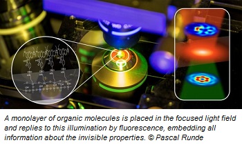
A team around physicist Prof. Dr. Cornelia Denz of the Institute of Applied Physics and chemist Prof. Dr. Bart Jan Ravoo of the Center for Soft Nanoscience (SoN) at the University of Münster successfully developed a nano-tomographic technique which is able to detect the typically invisible properties of nano-structured fields in the focus of a lens – without requiring any complex analysis algorithms or data post-processing. For this purpose, the team combined their knowledge in the field of nano-optics and organic chemistry to realize an approach based on a monolayer of organic molecules. This monolayer is placed in the focused light field and replies to this illumination by fluorescence, embedding all information about the invisible properties.
By the detection of this reply the distinct identification of the nano-field by a single, fast and straightforward camera image is enabled. “This approach finally opens the till now unexploited potential of these nano-structured light landscapes for many more applications,” says Cornelia Denz, who is heading the study. The study has been published in the journal “Nature Communications”.
Share on:


Suggested Items
Inkjet Solder Mask ‘Has Arrived’
04/10/2024 | Pete Starkey, I-Connect007I was delighted to be invited to attend an interactive webinar entitled “Solder Mask Coating Made Easy with Additive Manufacturing,” hosted by SUSS MicroTec Netherlands in Eindhoven. The webinar was introduced and moderated by André Bodegom, managing director at Adeon Technologies, and the speakers were Mariana Van Dam, senior product manager PCB imaging solutions at AGFA in Belgium; Ashley Steers, sales manager at Electra Polymers in the UK; and Dr. Luca Gautero, product manager at SUSS MicroTec Netherlands.
NetVia Group Acquires Direct Imaging from Mivatek
04/09/2024 | Miva TechnologiesMiva Technologies is pleased to announce NetVia Group, Irving, TX has acquired a new Miva 2400NG Dual Tray Direct Imaging System with 30-micron capabilities for inner, outer and soldermask imaging.
Teledyne to Acquire Adimec
02/13/2024 | TeledyneTeledyne Technologies Incorporated announced that it has entered into an agreement to acquire Adimec Holding B.V. and its subsidiaries.
Real Time with... productronica 2023: MivaTek Global Advances Technology With High-res Imaging System
12/08/2023 | Real Time with...productronicaMivaTek's Brendan Hogan talks about how the company employs Digitally Adaptive Rasterization Technology (DART) in their high-res imaging equipment. He also shares how the blurred line between semiconductors and microelectronics is driving broader application of the imaging process.
Keysight Enables Validation of Arbe 4D Imaging Radar Chipset
11/30/2023 | Keysight Technologies, Inc.Keysight Technologies, Inc. announces that Arbe has selected the E8719A Radar Target Solution (RTS) to test the Arbe 4D imaging radar chipset for automotive applications.