


 Marcy's Musings: The Growing Industry
 It’s Only Common Sense: Here’s What To Do After IPC APEX EXPO 2024
 Dan’s Biz Bookshelf: Seeing the How
Powering the Future: Smallest All-Digital Circuit Opens Doors to 5 NM Next-Gen Semiconductor
February 10, 2020 | Tokyo Institute of Technology, Socionext Inc.Estimated reading time: 3 minutes
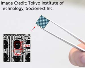
Scientists at Tokyo Institute of Technology (Tokyo Tech) and Socionext Inc. have designed the world's smallest all-digital phase-locked loop (PLL). PLLs are critical clocking circuits in virtually all digital applications, and reducing their size and improving their performance is a necessary step to enabling the development of next-generation technologies.
New or improved technologies, such as artificial intelligence, 5G cellular communications, and the Internet-of-Things, are expected to bring revolutionary changes in society. But for that to happen, high-performance system-on-a-chip (SoC)—a type of integrated circuit—devices are indispensable. A core building block of SoC devices is the phase-locked loop (PLL), a circuit that synchronizes with the frequency of a reference oscillation and outputs a signal with the same or higher frequency. PLLs generate 'clocking signals', whose oscillations act as a metronome that provides a precise timing reference for the harmonious operation of digital devices.
For high performance SoC devices to be realized, fabrication processes for semiconductor electronics must become more sophisticated. The smaller the area to implement digital circuitry is, the better the performance of the device. Manufacturers have been racing to develop increasingly smaller semiconductors. 7 nm semiconductors (a massive improvement over their 10 nm predecessor) are already in production, and methods to build 5 nm ones are now being looked at.
However, in this endeavor stands a major bottleneck. Existing PLLs require analog components, which are generally bulky and have designs that are difficult to scale down.
Scientists at Tokyo Tech and Socionext Inc., led by Prof. Kenichi Okada, have addressed this issue by implementing a 'synthesizable' fractional-N PLL, which only requires digital logic gates, and no bulky analog components, making it easy to adopt in conventional miniaturized integrated circuits.
Okada and team used several techniques to decrease the required area, power consumption and jitter—unwanted time fluctuations when transmitting digital signals—of their synthesizable PLLs. To decrease area, they employed a ring oscillator, a compact oscillator that can be easily scaled down. To suppress jitter, they reduced the phase noise—random fluctuations in a signal—of this ring oscillator, using 'injection locking'—the process of synchronizing an oscillator with an external signal whose frequency (or multiple of it) is close to that of the oscillator—over a wide range of frequencies. The lower phase noise, in turn, reduced power consumption.
The design of this synthesizable PLL beats that of all other current state-of-the-art PLLs in many important aspects. It achieves the best jitter performance with the lowest power consumption and smallest area (as can be seen in Figure 1). "The core area is 0.0036 mm2, and the whole PLL is implemented as one layout with a single power supply," remarks Okada. Further, it can be built using standard digital design tools, allowing for its rapid, low-effort, and low-cost production, making it commercially viable.
This synthesizable PLL can be easily integrated into the design of all-digital SoCs, and is commercially viable, making it valuable for developing the much sought after 5 nm semiconductor for cutting-edge applications including artificial intelligence, internet of things and many others, where high performance and low power consumption would be the critical requirements. But the contributions of this research go beyond these possibilities. "Our work demonstrates the potential of synthesizable circuits. With the design methodology employed here, other building blocks of SoCs, such as data converters, power management circuits, and wireless transceivers, could be made synthesizable as well. This would greatly boost design productivity and considerably reduce design efforts," explains Okada. Tokyo Tech and Socionext will continue their collaboration in this filed to advance the miniaturization of electronic devices, enabling the realization of newer-generation technologies.
This research work was conducted in cooperation with TeraPixel Technologies Inc.
Share on:


Suggested Items
Real Time with... IPC APEX EXPO 2024: Exploring IPC's PCB Design Courses with Kris Moyer
04/18/2024 | Real Time with...IPC APEX EXPOGuest Editor Kelly Dack and IPC instructor Kris Moyer discuss IPC's PCB design training and education offerings. They delve into course topics such as design fundamentals, mil/aero, rigid-flex, RF design, and advanced design concepts. They also highlight material selection for high-speed design, thermal management, and dissipation techniques. The interview wraps up with details about how to access these courses online.
Cadence Unveils Palladium Z3 and Protium X3 Systems
04/18/2024 | Cadence Design SystemsThe Palladium Z3 and Protium X3 systems offer increased capacity, and scale from job sizes of 16 million gates up to 48 billion gates, so the largest SoCs can be tested as a whole rather than just partial models, ensuring proper functionality and performance.
Signal Integrity Expert Donald Telian to Teach 'Signal Integrity, In Practice' Masterclass Globally
04/17/2024 | PRLOGDonald Telian and The EEcosystem announce the global tour of "Signal Integrity, In Practice," a groundbreaking LIVE masterclass designed to equip hardware engineers with essential skills for solving Signal Integrity (SI) challenges in today's fast-paced technological landscape.
On the Line With... Podcast Talks With Cadence Expert on Manufacturing
04/18/2024 | I-Connect007In “PCB 3.0: A New Design Methodology: Manufacturing” Patrick Davis returns to the podcast to talk about design rules. As design considerations become more and more complex, so, too, do the rulesets designers must abide by.
Designing Electronics for High Thermal Loads
04/16/2024 | Akber Roy, Rush PCB Inc.Developing proactive thermal management strategies is important in the early stages of the PCB design cycle to minimize costly redesign iterations. Here, I delve into key aspects of electronic design that hold particular relevance for managing heat in electronic systems. Each of these considerations plays a pivotal role in enhancing the reliability and performance of the overall system.