


 Marcy's Musings: The Growing Industry
 It’s Only Common Sense: Here’s What To Do After IPC APEX EXPO 2024
 Dan’s Biz Bookshelf: Seeing the How
Avicena Raises $25M in Series A to Fund Development of High Capacity microLED-based Optical Interconnects
August 2, 2022 | Business WireEstimated reading time: 1 minute
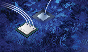
AvicenaTech Corp., the leader in microLED-based chip-to-chip interconnects, announced that the company has secured $25M in Series A funding from Samsung Catalyst Fund, Cerberus Capital Management, Clear Ventures, and Micron Ventures to drive the development of products based on Avicena’s breakthrough photonic I/O solution.
“We believe that Avicena technology can be transformational in unlocking compute-to-memory chip-to-chip high-speed interconnects. Such technology can be central to supporting future disaggregated architectures and distributed high-performance computing (HPC) systems,” said Marco Chisari, EVP of Samsung Electronics and Head of the Samsung Semiconductor Innovation Center.
“We are excited to participate in this round at Avicena,” said Amir Salek, Senior Managing Director at Cerberus Capital Management and former Head of Silicon for Google Infrastructure and Cloud. “Avicena has a highly differentiated technology addressing one of the main challenges in modern computer architecture. The technology offered by Avicena meets the needs for scaling future HPC and cloud compute networks and covers applications in conventional datacenter and 5G cellular networking.”
Avicena’s LightBundleTM I/O solution eliminates the existing bottlenecks of copper links triggered by power consumption, latency, reach and bandwidth density thus dramatically improving existing system performance. This enables new, dramatically higher-performing architectures in artificial intelligence (AI), machine learning (ML), cloud computing, next generation cellular radio, remote sensing, and aerospace applications.
The groundbreaking LightBundleTM technology is based on arrays of GaN micro-emitters that leverage the microLED display ecosystem and can be integrated onto any high-performance CMOS IC. Avicena leverages recent advances in the display industry to enable high volume, low-cost production of highly optimized microLED arrays.
“Avicena’s differentiated interconnect technology promises to enable next-generation high-performance processor and memory clusters,” said Gayathri Radhakrishnan, Senior Director at Micron Ventures. “Avicena represents a strategic investment opportunity for Micron Technology to support innovation in HPC architectures with our partners and customers.”
“We are excited about closing our Series A funding with a distinguished group of existing and new investors,” said Bardia Pezeshki, Founder and CEO of Avicena. “We will use the new funds to scale our team and build initial products for our growing family of partners and customers.”
Share on:


Suggested Items
Insulectro’s 'Storekeepers' Extend Their Welcome to Technology Village at IPC APEX EXPO
04/03/2024 | InsulectroInsulectro, the largest distributor of materials for use in the manufacture of PCBs and printed electronics, welcomes attendees to its TECHNOLOGY VILLAGE during this year’s IPC APEX EXPO at the Anaheim Convention Center, April 9-11, 2024.
ENNOVI Introduces a New Flexible Circuit Production Process for Low Voltage Connectivity in EV Battery Cell Contacting Systems
04/03/2024 | PRNewswireENNOVI, a mobility electrification solutions partner, introduces a more advanced and sustainable way of producing flexible circuits for low voltage signals in electric vehicle (EV) battery cell contacting systems.
Heavy Copper PCBs: Bridging the Gap Between Design and Fabrication, Part 1
04/01/2024 | Yash Sutariya, Saturn Electronics ServicesThey call me Sparky. This is due to my talent for getting shocked by a variety of voltages and because I cannot seem to keep my hands out of power control cabinets. While I do not have the time to throw the knife switch to the off position, that doesn’t stop me from sticking screwdrivers into the fuse boxes. In all honesty, I’m lucky to be alive. Fortunately, I also have a talent for building high-voltage heavy copper circuit boards. Since this is where I spend most of my time, I can guide you through some potential design for manufacturability (DFM) hazards you may encounter with heavy copper design.
Trouble in Your Tank: Supporting IC Substrates and Advanced Packaging, Part 5
03/19/2024 | Michael Carano -- Column: Trouble in Your TankDirect metallization systems based on conductive graphite or carbon dispersion are quickly gaining acceptance worldwide. Indeed, the environmental and productivity gains one can achieve with these processes are outstanding. In today’s highly competitive and litigious environment, direct metallization reduces costs associated with compliance, waste treatment, and legal issues related to chemical exposure. What makes these processes leaders in the direct metallization space?
AT&S Shines with Purest Copper on World Recycling Day
03/18/2024 | AT&SThe Styrian microelectronics specialist AT&S is taking World Recycling Day as an opportunity to review the progress that has been made in recent months at its sites around the world in terms of the efficient use of resources: