


 Marcy's Musings: The Growing Industry
 It’s Only Common Sense: Here’s What To Do After IPC APEX EXPO 2024
 Dan’s Biz Bookshelf: Seeing the How
Wafer-scale Quantum Devices Closer to Reality through Spintronics
June 26, 2015 | University of ChicagoEstimated reading time: 2 minutes
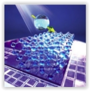
An electronics technology that uses the “spin”—or magnetization—of atomic nuclei to store and process information promises huge gains in performance over today’s electron-based devices. But getting there is proving challenging.
Now, researchers at the University of Chicago’s Institute for Molecular Engineering have made a crucial step toward nuclear spintronic technologies. They have gotten nuclear spins to line themselves up in a consistent, controllable way, and they have done it using a high-performance material that is practical, convenient and inexpensive.
“Our results could lead to new technologies like ultra-sensitive magnetic resonance imaging, nuclear gyroscopes and even computers that harness quantum mechanical effects,” said Abram Falk, the lead author of the report on the research, which was featured as the cover article of the June 17 issue of Physical Review Letters. Falk and colleagues in David Awschalom’s IME research group invented a new technique that uses infrared light to align spins. They did so using silicon carbide, an industrially important semiconductor.
Nuclear spins tend to be randomly oriented. Aligning them in a controllable fashion is usually a complicated and only marginally successful proposition. The reason, explains Paul Klimov, a co-author of the paper, is that “the magnetic moment of each nucleus is tiny, roughly 1,000 times smaller than that of an electron.”
This small magnetic moment means that little thermal kicks from surrounding atoms or electrons can easily randomize the direction of the nuclear spins. Extreme experimental conditions such as high magnetic fields and cryogenic temperatures (-238 degrees Fahrenehit and below) are usually required to get even a small number of spins to line up. In magnetic resonance imaging, for example, only one to 10 out of a million nuclear spins can be aligned and seen in the image, even with a high magnetic field applied.
Using their new technique, Awschalom, the Liew Family Professor in Spintronics and Quantum Information, and his associates aligned more than 99 percent of spins in certain nuclei in silicon carbide. Equally important, the technique works at room temperature—no cryogenics or intense magnetic fields needed. Instead, the research team used light to “cool” the nuclei.
While nuclei do not interact with light themselves, certain imperfections, or “color-centers,” in the SiC crystals do. The electron spins in these color centers can be readily optically cooled and aligned, and this alignment can be transferred to nearby nuclei. Had the group tried to achieve the same degree of spin alignment without optical cooling, they would have had to chill the SiC chip physically to just five millionths of a degree above absolute zero (-459.6 degrees Fahrenheit).
Getting spins to align in room-temperature silicon carbide brings practical spintronic devices a significant step closer, said Awschalom. The material is already an important semiconductor in the high-power electronics and opto-electronics industries. Sophisticated growth and processing capabilities are already mature. So prototypes of nuclear spintronic devices that exploit the IME researchers’ technique may be developed in the near future.
“Wafer-scale quantum technologies that harness nuclear spins as subatomic elements may appear more quickly than we anticipated,” Awschalom said.
Share on:


Suggested Items
Inkjet Solder Mask ‘Has Arrived’
04/10/2024 | Pete Starkey, I-Connect007I was delighted to be invited to attend an interactive webinar entitled “Solder Mask Coating Made Easy with Additive Manufacturing,” hosted by SUSS MicroTec Netherlands in Eindhoven. The webinar was introduced and moderated by André Bodegom, managing director at Adeon Technologies, and the speakers were Mariana Van Dam, senior product manager PCB imaging solutions at AGFA in Belgium; Ashley Steers, sales manager at Electra Polymers in the UK; and Dr. Luca Gautero, product manager at SUSS MicroTec Netherlands.
NetVia Group Acquires Direct Imaging from Mivatek
04/09/2024 | Miva TechnologiesMiva Technologies is pleased to announce NetVia Group, Irving, TX has acquired a new Miva 2400NG Dual Tray Direct Imaging System with 30-micron capabilities for inner, outer and soldermask imaging.
Teledyne to Acquire Adimec
02/13/2024 | TeledyneTeledyne Technologies Incorporated announced that it has entered into an agreement to acquire Adimec Holding B.V. and its subsidiaries.
Real Time with... productronica 2023: MivaTek Global Advances Technology With High-res Imaging System
12/08/2023 | Real Time with...productronicaMivaTek's Brendan Hogan talks about how the company employs Digitally Adaptive Rasterization Technology (DART) in their high-res imaging equipment. He also shares how the blurred line between semiconductors and microelectronics is driving broader application of the imaging process.
Keysight Enables Validation of Arbe 4D Imaging Radar Chipset
11/30/2023 | Keysight Technologies, Inc.Keysight Technologies, Inc. announces that Arbe has selected the E8719A Radar Target Solution (RTS) to test the Arbe 4D imaging radar chipset for automotive applications.