


 Marcy's Musings: The Growing Industry
 It’s Only Common Sense: Here’s What To Do After IPC APEX EXPO 2024
 Dan’s Biz Bookshelf: Seeing the How
Supercool Electrons
January 25, 2017 | OISTEstimated reading time: 3 minutes
The future of quantum computing is a hot topic not only for experts but also in many commercial and governmental agencies. Rather than processing and storing information as bits in transistors or memories, which limit information to the binary “1” or “0”, quantum computers would instead use quantum systems, such as atoms, ions, or electrons, as “qubits” to process and store “quantum information” in, which can be in an infinite number of combinations of “1 and 0”. Large technology corporations, such as Google, Microsoft, Intel, and IBM are investing heavily in related projects that may lead to realize the quantum computer and technologies. At the same time, universities and research institutes around the world are researching novel quantum systems, adoptable for quantum computing. The Quantum Dynamics Unit at the Okinawa Institute of Science and Technology Graduate University (OIST), has recently made novel findings about electrons floating on the surface of liquid helium, a quantum system which may be a new candidate for quantum computing into reality. These results were published in Physical Review B.
One of the common problems in quantum computing research using solids is that it is very difficult to make perfectly identical qubits because intrinsic defects or impurities in the materials used randomly affect each individual qubit performance. “Our motivation for pursuing a liquid helium system is that it is intrinsically pure and free of defects, which theoretically allows for the creation of perfectly identical qubits. Additionally, we can move electrons in this liquid helium system, which is difficult or nearly impossible in other quantum systems,” explained Prof. Denis Konstantinov, head of the Quantum Dynamics Unit. Therefore, it is believed that adopting this system for quantum computing might bring the whole field to the next level.
Utilizing electrons on a liquid helium surface for quantum computing requires isolating individual electrons on a helium surface and controlling their quantum degrees of freedom, either motional or spin. It may also require the movement of electrons to different locations, thus it is also important to understand the physics of the interaction between electrons and the helium surface. It was previously discovered that electrons on helium can form a two-dimensional crystal, and some unique phenomena occur when this crystal moves along the helium surface, due to the interaction between electrons and surface waves. The OIST scientists, however, are the first to probe how these phenomena depend on the size of the electron crystal. To test this, Dr. Alexander Badrutdinov, Dr. Oleksandr Smorodin and OIST PhD student Jui-Yin Lin, built a microscopic channel device that contained an electron trap within to isolate a crystal of a relatively small number of electrons. This crystal would then be moved across the liquid helium surface by altering electrostatic potential of one of the device electrodes. This motion would be detected by measuring image charges, which are induced by the moving electrons, flowing through another electrode using a commercially available current amplifier and lock-in detector.
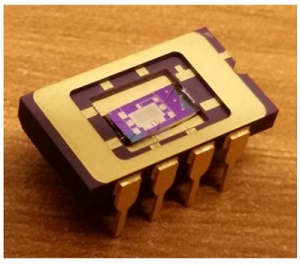
Images of the electron trap architecture. Top: Schematic representation of the experiment. Current of surface electrons, induced by ac voltage applied to the electrode underneath Reservoir 1, flows between Reservoirs 1 and 4 through the central microchannel, as shown by the red arrow. Middle: Cross section of the central microchannel around the trap area. Bottom: Photograph of the microchannel device on a copper sample cell, with subsequent close-up photographs of the central channel and surrounding reservoirs.
“This research gave us some insights into the physics of the interaction between electrons and the helium surface, as well as expanded our micro-engineering capabilities” states Dr. Alexander Badrutdinov, a former member of the Quantum Dynamics Unit and the first author of the paper. “We successfully adopted a technology to confine electrons into microscopic devices, on the scale of few microns. With this technology we studied the motion of microscopic two-dimensional electron crystals along a liquid helium surface and saw no difference between the movement of large electron crystals, on the scale of millions to billions of electrons, and crystals as small as a few thousands of electrons, when theoretically, differences should exist”.
This research is the first step at OIST in the prospect of using this system for quantum computing. According to Konstantinov, “the next step in this research is to isolate an even smaller electron crystal, and ultimately, a single electron, and to move them in this system. Unlike other systems, this system has the potential to be a pure, scalable system with mobile qubits.” In theory, this type of system would have the potential to revolutionize the quantum computing research field.
Share on:


Suggested Items
Insulectro’s 'Storekeepers' Extend Their Welcome to Technology Village at IPC APEX EXPO
04/03/2024 | InsulectroInsulectro, the largest distributor of materials for use in the manufacture of PCBs and printed electronics, welcomes attendees to its TECHNOLOGY VILLAGE during this year’s IPC APEX EXPO at the Anaheim Convention Center, April 9-11, 2024.
ENNOVI Introduces a New Flexible Circuit Production Process for Low Voltage Connectivity in EV Battery Cell Contacting Systems
04/03/2024 | PRNewswireENNOVI, a mobility electrification solutions partner, introduces a more advanced and sustainable way of producing flexible circuits for low voltage signals in electric vehicle (EV) battery cell contacting systems.
Heavy Copper PCBs: Bridging the Gap Between Design and Fabrication, Part 1
04/01/2024 | Yash Sutariya, Saturn Electronics ServicesThey call me Sparky. This is due to my talent for getting shocked by a variety of voltages and because I cannot seem to keep my hands out of power control cabinets. While I do not have the time to throw the knife switch to the off position, that doesn’t stop me from sticking screwdrivers into the fuse boxes. In all honesty, I’m lucky to be alive. Fortunately, I also have a talent for building high-voltage heavy copper circuit boards. Since this is where I spend most of my time, I can guide you through some potential design for manufacturability (DFM) hazards you may encounter with heavy copper design.
Trouble in Your Tank: Supporting IC Substrates and Advanced Packaging, Part 5
03/19/2024 | Michael Carano -- Column: Trouble in Your TankDirect metallization systems based on conductive graphite or carbon dispersion are quickly gaining acceptance worldwide. Indeed, the environmental and productivity gains one can achieve with these processes are outstanding. In today’s highly competitive and litigious environment, direct metallization reduces costs associated with compliance, waste treatment, and legal issues related to chemical exposure. What makes these processes leaders in the direct metallization space?
AT&S Shines with Purest Copper on World Recycling Day
03/18/2024 | AT&SThe Styrian microelectronics specialist AT&S is taking World Recycling Day as an opportunity to review the progress that has been made in recent months at its sites around the world in terms of the efficient use of resources: