


 Marcy's Musings: The Growing Industry
 It’s Only Common Sense: Here’s What To Do After IPC APEX EXPO 2024
 Dan’s Biz Bookshelf: Seeing the How
Red, Green, Yellow, Blue …
August 7, 2017 | LMUEstimated reading time: 1 minute
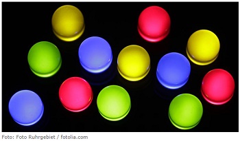
The color of the light emitted by an LED can be tuned by altering the size of their semiconductor crystals. LMU researchers have now found a clever and economical way of doing just that, which lends itself to industrial-scale production.
Unlike our old friend the incandescent lightbulb, light-emitting diodes (or LEDs) produce light of a defined color within the spectral range from the infrared to the ultraviolet. The exact wavelength of the emission is determined by the chemical composition of the semiconductor employed, which is the crucial component of these devices. In the case of some semi-conducting materials, the color can also be tuned by appropriately modifying the size of the crystals of which the light-emitting layer is composed. In crystals with dimensions on the order of a few nanometers, quantum mechanical effects begin to make themselves felt.
LMU researchers in collaboration with colleagues at the University of Linz (Austria) have now developed a method for the production of semi-conducting nanocrystals of defined size based on the cheap mineral oxide known as perovskite. These crystals are extremely stable, which ensures that the LEDs exhibit high color fidelity – an important criterion of quality. Moreover, the resulting semiconductors can be printed on suitable surfaces, and are thus predestined for the manufacture of LEDs for use in displays.
The crucial element in the new method is a thin wafer, only a few nanometers thick, which is patterned like a waffle. The depressions serve as tiny reaction vessels, whose shape and volume ultimately determine the final size of the nanocrystals. “Optimal measurements of the size of the crystals were obtained using a fine beam of high-energy X-radiation at the Deutsche Elektronen-Synchrotron (DESY) in Hamburg“, says LMU researcher Dr. Bert Nickel, member of the Nanosystems Initiative Munich (NIM), a Cluster of Excellence.
Moreover, the wafers are produced by means of an economical electrochemical process, and can be fashioned directly into LEDs. “Our nanostructure oxide layers also prevent contact between the semiconductor crystals and deleterious environmental factors such as free oxygen and water, which would otherwise limit the working lifetime of the LEDs,” as Dr. Martin Kaltenbrunner of the Johannes Kepler University in Linz explains. In the next step, we want to enhance the efficiency of these diodes further, and explore their potential for use in other applications, such as flexible displays.
Share on:


Suggested Items
Connect the Dots: Best Practices for Prototyping
09/21/2023 | Matt Stevenson -- Column: Connect the DotsPCB prototyping is a critical juncture during an electronic device’s journey from concept to reality. Regardless of a project’s complexity, the process of transforming a design into a working board is often enlightening in terms of how a design can be improved before a PCB is ready for full production.
The Drive Toward UHDI and Substrates
09/20/2023 | I-Connect007 Editorial TeamPanasonic’s Darren Hitchcock spoke with the I-Connect007 Editorial Team on the complexities of moving toward ultra HDI manufacturing. As we learn in this conversation, the number of shifting constraints relative to traditional PCB fabrication is quite large and can sometimes conflict with each other.
Asia/Pacific AI Spending Surge to Reach a Projected $78 Billion by 2027
09/19/2023 | IDCAsia/Pacific spending on Artificial Intelligence (AI) ), including software, services, and hardware for AI-centric systems will grow to $78.4 billion in 2027, according to International Data Corporation's latest Worldwide Artificial Intelligence Spending Guide.
Intel to Sell Minority Stake in IMS Nanofabrication Business to TSMC
09/13/2023 | IntelIntel Corporation announced that it has agreed to sell an approximately 10% stake in the IMS Nanofabrication business to TSMC. TSMC’s investment values IMS at approximately $4.3 billion, consistent with the valuation of the recent stake sale to Bain Capital Special Situations.
RAF Invests in BAE Systems’ Most Advanced Fighter Pilot Helmet
09/13/2023 | BAE SystemsThe UK Ministry of Defence (MOD) has awarded BAE Systems a contract to develop its Striker II Helmet Mounted Display (HMD) for the Royal Air Force (RAF) Typhoon fleet. The contract, valued at £40m, will create and sustain more than 200 highly-skilled jobs at BAE Systems’ sites in Kent and Lancashire working directly on the Striker II programme. In total, the Typhoon programme sustains more than 20,800 jobs across the UK.