


 Marcy's Musings: The Growing Industry
 It’s Only Common Sense: Here’s What To Do After IPC APEX EXPO 2024
 Dan’s Biz Bookshelf: Seeing the How
ESI Unveils Newest Addition to Its PCB Via Drilling Product Portfolio
December 7, 2015 | ESIEstimated reading time: 1 minute
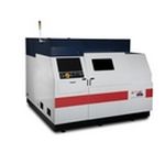
Electro Scientific Industries, Inc., an innovator of laser-based manufacturing solutions for the micromachining industry, today introduced its nViant™ laser processing system designed for High-Density Interconnect (HDI) applications. The nViant™ system expands ESI's portfolio of solutions for the Printed Circuit Board (PCB) industry. This portfolio already includes the industry-leading 5335 family of tools for flexible printed circuit via drilling as well as the CornerStone™ via drilling system for manufacturing high accuracy substrates used for integrated circuits.
A CO2 laser-based microvia drilling system, nViant™ combines excellent quality via formation with industry-leading accuracy on a robust platform that delivers high throughput at a competitive price point. The nViant™ system was designed and built for manufacturers of HDI boards, used in smartphones, wearables and other mobile devices. HDI components are also used in industrial and automotive markets.
High-volume manufacturing of HDI PCBs requires blind (BHV) and through-hole (LTH) via processing; these vias are typically created with laser drills, which offer fast, reliable, and cost-effective processing at a miniaturized scale. The nViant™ system enables HDI manufacturers to drill vias in a broad range of copper-clad base materials such as glass-woven reinforced epoxy resins (FR4) or other specialty materials. The nViant™ system joins ESI's long history of products targeted for the production floor and reinforces ESI's focus and experience on speed, quality and accuracy.
"nViant™ leverages our expertise in laser processing and our proven track record of success in laser-based systems—especially in the flexible PCB manufacturing segment, where ESI is the clear market leader—and applies it to the HDI manufacturing segment," said Chris Ryder, Director of HDI Product Management at ESI. "The nViant™ system delivers a compelling solution for HDI PCB manufacturers. It's engineered to provide great reliability at high-quality output with the industry's lowest cost of ownership, and is backed by ESI's professional service and support organization with local offices throughout the world."
For PCB manufacturers of HDI boards, CO2 laser processing is the optimal choice for overall lower cost of ownership. ESI's nViant™ system extends this advantage with robust platform construction that allows for 24/7 operation. Support is provided through ESI's professional service organization.
The launch of nViant™ is taking place in conjunction with the 2015 International Printed Circuit & APEX South China Fair (2015 HKPCA & IPC Show) December 2-4 at the Shenzhen Convention and Exhibition Center in Shenzhen, China.
Share on:


Suggested Items
Insulectro’s 'Storekeepers' Extend Their Welcome to Technology Village at IPC APEX EXPO
04/03/2024 | InsulectroInsulectro, the largest distributor of materials for use in the manufacture of PCBs and printed electronics, welcomes attendees to its TECHNOLOGY VILLAGE during this year’s IPC APEX EXPO at the Anaheim Convention Center, April 9-11, 2024.
ENNOVI Introduces a New Flexible Circuit Production Process for Low Voltage Connectivity in EV Battery Cell Contacting Systems
04/03/2024 | PRNewswireENNOVI, a mobility electrification solutions partner, introduces a more advanced and sustainable way of producing flexible circuits for low voltage signals in electric vehicle (EV) battery cell contacting systems.
Heavy Copper PCBs: Bridging the Gap Between Design and Fabrication, Part 1
04/01/2024 | Yash Sutariya, Saturn Electronics ServicesThey call me Sparky. This is due to my talent for getting shocked by a variety of voltages and because I cannot seem to keep my hands out of power control cabinets. While I do not have the time to throw the knife switch to the off position, that doesn’t stop me from sticking screwdrivers into the fuse boxes. In all honesty, I’m lucky to be alive. Fortunately, I also have a talent for building high-voltage heavy copper circuit boards. Since this is where I spend most of my time, I can guide you through some potential design for manufacturability (DFM) hazards you may encounter with heavy copper design.
Trouble in Your Tank: Supporting IC Substrates and Advanced Packaging, Part 5
03/19/2024 | Michael Carano -- Column: Trouble in Your TankDirect metallization systems based on conductive graphite or carbon dispersion are quickly gaining acceptance worldwide. Indeed, the environmental and productivity gains one can achieve with these processes are outstanding. In today’s highly competitive and litigious environment, direct metallization reduces costs associated with compliance, waste treatment, and legal issues related to chemical exposure. What makes these processes leaders in the direct metallization space?
AT&S Shines with Purest Copper on World Recycling Day
03/18/2024 | AT&SThe Styrian microelectronics specialist AT&S is taking World Recycling Day as an opportunity to review the progress that has been made in recent months at its sites around the world in terms of the efficient use of resources: