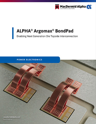
Enabling Next-Generation Die Topside Interconnection (Power Electronics)
Author: MacDermid Alpha Electronics Solutions
This white paper introduces ALPHA® Argomax® BondPad, a next-generation sinter-ready copper foil solution for advanced semiconductor die topside interconnection, emphasizing improved reliability, thermal performance, and manufacturing simplicity for high-power and miniaturized electronic applications.