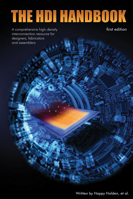
The widespread use of new electronic components employing Ball-Grid Array (BGA), Chip Scale Packaging (CSP), and other evolving technology form-factors means new fabrication techniques must be used to create printed circuit boards (PCBs) that will accommodate parts with extremely tight lead pitches and small geometries. In addition, extremely fast signal rise-times and signal bandwidths challenge systems designers to find better ways to overcome the negative effects of inductance, noise, radio frequency interference (RFI) and electro-magnetic interference (EMI) have on their product’s performance. The use of PCBs incorporating microvia circuit interconnects is currently one of the most viable solutions on the market.
ISBN: 978-0-9796189-1-8
Edited by: Happy Holden
Happy Holden is the retired director of electronics and innovations for GENTEX Corporation. Formerly, he was the chief technical officer for the world’s largest PCB fabricator—Hon Hai Precision Industries (Foxconn). Prior to Foxconn, Holden was the senior PCB technologist for Mentor Graphics and advanced technology manager at Nan Ya/Westwood Associates and Merix. He previously worked at Hewlett-Packard for over 28 years as director of PCB R&D and manufacturing engineering manager. He has been involved in advanced PCB technologies for over 47 years.
Contributing authors: Happy Holden, John Andresakis, Eric Bogatin, Michael Carano, Karen Carpenter, Karl H. Dietz, Mark Laing, Christophe Vaucher, Per Viklund, Matt Wuensch
Chapter Summaries
-
Chapter 1
Introduction
The widespread use of new electronic components employing Ball-Grid Array (BGA), Chip Scale Packaging (CSP), and other evolving technology form-factors means new fabrication techniques must be used to create printed circuit boards (PCBs) that will accommodate parts with extremely tight lead pitches and small geometries. In addition, extremely fast signal rise-times and signal bandwidths challenge systems designers to find better ways to overcome the negative effects of inductance, noise, radio frequency interference (RFI) and electro-magnetic interference (EMI) have on their product’s performance. The use of PCBs incorporating microvia circuit interconnects is currently one of the most viable solutions on the market.
-
Chapter 2
The Interconnect Market
HDI products, size and market growth rates, examples of different HDI products using the four Platforms: 1. Consumer and mobile phones, 2. substrates 3. Modules and 4. large-high performance boards. History of adoption and world-wide capacity and pricing.
-
Chapter 3
Design of Advanced Substrates
As the electronic products industry continues to push the envelope of extreme miniaturization, product developments teams are being forced further into the realm of high density interconnect. Design techniques and substrates labeled exotic only a few short years ago are now considered mainstream. In particular, build-up substrate usage has grown dramatically, and is now found in a large percentage of high production electronic products. This Section is to educate and inform you on the technologies, needs, issues and solutions available today for advanced substrate design. The focus will briefly cover the 4 changes to TH PCB design techniques required for HDI and the IPC Design Standard 2226.
-
Chapter 4
Electrical Performance
The good old days of 10 to 16 MHz clock frequencies are gone. It used to be the chief design challenge in circuit boards or packages was routing all the signals in two layers and getting packages that wouldn’t crack during assembly. The electrical properties of the interconnects were not important because they didn’t affect system performance. But the world has changed in the past 10 years. Clock frequencies on chip now are over 3 GHz, and on board, are over 800 MHz. In most systems, as the clock frequency goes up, the rise time always gets shorter. A shorter rise time means signal integrity problems increase dramatically. Signal integrity is broadly concerned with the problems that arise from how the electrical properties of the interconnects and power distribution affect system performance. External signals can affect noise as well as the return path for signals along planes. HDI provides miniaturization, smaller and shorter vias, shorter interconnect lengths with smaller parts and finer pitch devices, thinner and lower dielectric-laser drillable dielectrics and embedded components. These can be enabling techniques for improved high-frequency electrical performance.
-
Chapter 5
Materials
This chapter will list the major types of materials used to make printed circuit boards and in particular those used to make HDI boards. It will also include a small section on materials for embedded passives/actives as HDI is an enabler for many embedded passive/active applications.
-
Chapter 6
The HDI Mfg Processes
Various HDI mfg processes and structures are explained. These utilize standard PCB processes but with greater miniaturization and higher density.
-
Chapter 7
Small Hole Creation
This chapter will cover key via formation technologies including laser via formation and, where appropriate, mechanical drilling.
-
Chapter 8
Metalization
Desmear & metalization (electroless), including the materials and processes for paste in vias
-
Chapter 9
Fine-Line Imaging and Etching
Image transfer processes, stripping & etching fine lines, registration, equipment, and materials for fine-line image transfer.
-
Chapter 10
Via-fill, Plating and Finishes
Plating, pulse-plating, small-holes plating and filling, final finishes
-
Chapter 11
Inspection and Testing
Inspection, AOI, and electrical testing of HDI
-
Chapter 12
Quality, Acceptability & Reliability
Performance of HDI Benchmarking, Vendor readiness, qualification, quality issues, lab techniques and equipment.
-
Chapter 13
Assembly and Test Processes for HDI PCBs
This chapter will cover the Assembly and Test processes that are impacted by an HDI PCB. This will cover the production processes starting from a completed, fabricated PCB and finishing with parts being attached to the bare PCB. It will not cover processes that are affected during the fabrication of the bare PCB. It will also cover the schematic and layout stages of PCB design where it is impacted by the eventual assembly and test process.
-
Chapter 14
Embedded Components
Embedded Resistors, Embedded Capacitors, Distributed capacitance and Embedded Actives, the materials and design tools.
-
Chapter 15
Advanced HDI and Next Generation Interconnects
The purpose of this chapter is to examine a variety of advanced HDI fabrication processes that have evolved over time, plus an exploration of how next-generation HDI technologies will continue to evolve and become smaller, following integrated circuit cell geometries.
-
Chapter 16
Advanced Packaging and System-in-Packages
Traditional silicon packaging is evolving to 3-D/stacked dies and multiple-components as in System-in-Package (SiP). Current trends leading to a higher level of 3-D integration create big challenges for design tools, methodologies, and the individual designer.


