FEATURED NEWS AND INFORMATION:


Send your news item to: news@iconnect007.com
Breaking News: What’s Next for PCB Materials? I-Connect007 Podcast Series Turns to Supply Chain Resilience
I-Connect007 continues its six-part podcast series with Isola experts titled, PCB Materials: The Backbone and Future of Electronics, with the...
April Issue of I-Connect007 Magazine: Beyond the Rulebook
In this month’s I-Connect007 Magazine, we asked PCB designers, fabricators, and suppliers what it really means to operate without a rulebook. Their...
I-Connect007 Releases Episode 4 of ‘PCB Materials: The Backbone and Future of Electronics’ Podcast Series
I-Connect007 is excited to announce the release of Episode 4 in its six-part podcast series with Isola experts, PCB Materials: The Backbone and...
ASC Sunstone Circuits Implements Smart Parts Technology at Mulino Facility to Enhance PCB Manufacturing Efficiency
ASC Sunstone Circuits, a division of American Standard Circuits, has implemented Smart PartsTM Classics technology at its Mulino, Oregon,...
Global Electronics Association Announces New Board Members at APEX EXPO 2026
At the 69th Global Electronics Association Annual Meeting on March 17, held in conjunction with APEX EXPO 2026, the Association’s Board of...
Click Here for More News
Send your news item to: news@iconnect007.com
Click here for press release tips
FEATURED ARTICLES AND COLUMNS:

MORE ARTICLES
Applications, Challenges, and the Future of Flex–Packaging Integration, Part 2
April 16, 2026 | Anaya Vardya, American Standard Circuits
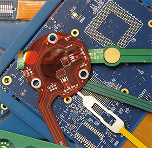
In the second of this two-part series, Anaya Vardya of American Standard Circuits examines applications, challenges, manufacturing considerations, and future trends emerging from the convergence of flexible printed circuit boards and advanced semiconductor packaging. Applications driving the convergence include consumer electronics, automotive systems, medical, wearables, aerospace and more.
MORE ARTICLES
Testimonial
"In a year when every marketing dollar mattered, I chose to keep I-Connect007 in our 2025 plan. Their commitment to high-quality, insightful content aligns with Koh Young’s values and helps readers navigate a changing industry. "
Beyond the Rulebook Featuring:
- Marcy’s Musings: Operating Without a Rulebook by Marcy LaRont
- The Chemical Connection: When the Industry Moves Faster Than the Standards by Don Ball
- Jiva Soluboard Getting the Attention It Deserves with Stephen Driver
- Trouble in Your Tank: In Complex Systems, Design Rules Aren’t Optional by Michael Carano
- Designing Without a Rulebook: When Engineering Becomes Innovation by Stephen V. Chavez
Copyright © I-Connect007 | IPC Publishing Group Inc. All rights reserved.
Log in


