


 Flexible Thinking: PCB Designers Still Wanted
 Connect the Dots: Five Best Practices for Designing Flex and Rigid-flex PCBs
 Tim’s Takeaways: Human Ingenuity and the Rigid-flex PCB
Inkjet Printable and Biocompatible Layered Electronics
March 29, 2017 | Graphene FlagshipEstimated reading time: 4 minutes
Printed electronics can lead to both low-cost and flexible devices. Flexible electronics is of particular interest for wearable systems, such as health and fitness trackers, while the relative low-costs of printing are attractive for functional packaging for consumer products. Graphene and related layered materials (GRMs) are ideal for printed electronics because they can be readily solution processed into inks that have excellent electronic properties.
In a step toward rapid and low-cost prototyping of electronic devices, researchers from the Graphene Flagship have demonstrated fully inkjet printed programmable memory devices, using biocompatible water-based inks.
Now, biocompatible, water-based inks containing GRMs have been developed as building blocks for inkjet printable electronic devices. Importantly, the inks can be used to successfully inkjet print electronic devices based on combinations of different layered materials. The research, published in Nature Nanotechnology, was performed in a collaboration between researchers at the University of Manchester, UK and the University of Pisa, Italy.
Inkjet printing
The GRM inks containing conductive graphene, the insulator hexagonal boron nitride (hBN) and semiconductor transition metal dichalcogenides (TMDs), such as MoS2 and WS2, provide the full range of electronic properties needed to print complex electronics, including photodetectors. The inks can be printed onto flexible and stiff substrates, such as paper, glass and plastic, and the inks’ biocompatibility also suggests possibilities for printing biomedical devices such as sensor implants.
Inkjet printing is attractive as a fast and accessible route to printed electronics, because of simple switching of design and materials. The devices were produced using a material inkjet printer available in the market, demonstrating the suitability of this technique as a platform for rapid prototyping (similar to 3D printing), while paving the way towards print-on-demand electronics.
Gianluca Fiori, a researcher at the department of Information Engineering at the University of Pisa, Italy, said “We are now entering a new scenario in the field of electronics, where electronic systems can be printed on demand and on flexible substrates as paper. GRMs based inks could indeed represent an enabling technology for the fast-growing market of flexible and portable electronics.”
Printed memory
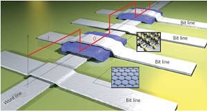
The inks were used to print photodetectors and the first inkjet printable read-only memory, in the form of an array of bit-strips using graphene and WS2 inks. Such readable memory could be ideal for identification numbers in radio-frequency identification (RFID) tags, and could be developed further into more complex memory systems when integrated with other printed devices such as diodes and transistors.
Heterostructures, made of stacked layers of different materials, are important for compact integration of functional circuits. Typically, with inkjet printing it is very difficult to obtain good interfaces, meaning the printed devices do not operate reliably. For these new inks, the researchers optimised the ink formula specifically for inkjet printing, adding xantham gum as a binder to prevent the printed interfaces merging together.
The research was led by Cinzia Casiraghi, a researcher in the School of Chemistry at the University of Manchester, UK. She explained that the printable heterostructures are “the first step towards the realization of low-cost and flexible devices.” Outlining the challenges that this research overcomes, she said “Currently, heterostructures are formed by two or three layers and only very few examples of more complex heterostructures have been demonstrated, using non-scalable techniques. We are now in the position to fabricate devices of arbitrary geometry on a flexible substrate. For example, we can produce arrays of heterostructures, where every junction can be designed ad hoc to store or sense a particular type of information.”
A printed future
One important area where these printed circuits could find application is in smart packaging. The Internet of Things is enabling connectivity in an unprecedented range of applications, and smart packaging could be ideal for managing inventories and monitoring spoilage in food, drinks and pharmaceuticals; applications for which the ink’s biocompatibility is essential. “We are also very excited about the possibility of implementing logic circuits made of these materials – indeed, we are further developing these type of devices,” added Casiraghi.
Coşkun Kocabaş, a researcher at Bilkent University, Turkey, is Deputy Leader of the Partnering Division of the Graphene Flagship, where Casiraghi's ERC project NOC2D is affiliated. “This method provides the advantage of heterogeneous integration of conducting, semiconducting and dielectric layered materials. This capability will enable new directions in electronics aiming to generate very large scale and low cost circuits,” he said. “Another exciting next step would be integration of this method with 3D printing techniques which could enable printed circuits with exotic topologies.”
Andrea Ferrari, Science and Technology Officer and Chair of the Management Panel of the Graphene Flagship added "Printed and flexible electronics has been at the core of the Graphene Flagship since its beginning and is certainly one of the key areas where graphene and related materials can find near-term applications. This work is an important step forward, and demonstrates the successful collaboration of between the Flagship Core 1 Partners and the newly formed partnering division, further strengthening the Flagship as the European hub for innovation in graphene and related materials."
Share on:


Suggested Items
Electronics Industry Sentiment Rose in April, Hitting New High
05/02/2024 | IPCApril 2024 marked the third consecutive month of sentiment growth among electronics manufacturers. When asked if they expected labor costs for hourly workers to rise over the next month, manufacturers in the United States, Mexico, and Europe predicted a five percent increase, while manufacturers in Asia predicted a slightly lower four percent increase.
iNEMI Names Grace O'Malley CTO
05/02/2024 | iNEMIThe Board of Directors of the International Electronics Manufacturing Initiative (iNEMI) has named Grace O'Malley Chief Technical Officer (CTO).
ZESTRON Academy Launches 2024 Advanced Packaging & Power Electronics Webinar Series
05/01/2024 | ZESTRONZESTRON, the leading global provider of high-precision cleaning products, services, and training solutions in the electronics manufacturing and semiconductor industries, proudly announces the launch of its highly anticipated webinar series on Advanced Packaging & Power Electronics, a webinar series on the latest innovations, cleaning, and corrosion challenges.
NextFlex Convenes the Hybrid Electronics Community at Binghamton University
05/01/2024 | NextFlexBinghamton University hosted the NextFlex hybrid electronics community on April 18 for a day of expert presentations, breakout sessions on technology and manufacturing topics, and networking.
HQ NextPCB of HQ Electronics Debut on the International Stage for Electronics Manufacture at IPC APEX 2024
05/01/2024 | PRNewswireHQ NextPCB of HQ Electronics, a leading Chinese-based multilayer PCB manufacturer and assembly house showcased its industrial prowess on the international stage for the first time at the IPC APEX Expo 2024.