


 Flexible Thinking: PCB Designers Still Wanted
 Connect the Dots: Five Best Practices for Designing Flex and Rigid-flex PCBs
 Tim’s Takeaways: Human Ingenuity and the Rigid-flex PCB
Part 2: EIPC’s Winter Conference in Lyon, France: Day 2 Review
February 21, 2018 | Pete Starkey, I-Connect007Estimated reading time: 9 minutes
Christoph Bornhorn, managing director of FED (Fachverband Elektronik-Design), the German association for design, PCB and electronics manufacturing, described how FED had developed a four-stage training programme known as ZED (Zertifizierter Elektronik Designer)—Certified Electronic Designer—with the objective of increasing the professional competence and acceptance of PCB designers. Since the programme had begun in 2015, more than 500 people had participated in courses and seminars and gained basic and specialised knowledge of PCB design. A key principle of the programme was to involve designers in the entire electronics process and to gain an understanding of electrical engineering and physics, manufacturing technology and testing procedures, materials science, standards and regulations, and economic aspects, as well as studying PCB design from first principles.
At each of the four stages, participants who passed the exam received a qualification certificate for that ZED level. After passing the whole programme they were entitled to hold the title Zertifizierter Elektronik-Designer, ZED. So far, 22 people had passed the final exams at Level 4, and FED considered the ZED concept a major success. The intention was to intensify the marketing effort to bring the programme to the attention of a wider public and recruit more participants. At present, the programme was available only in German language.
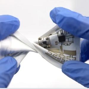
The opening slide announced, “A New Era of Agile Electronics,” as Nano Dimension’s materials manager Robert Even explored the challenges of 3D-printed electronics and discussed how this disruptive technology would redefine PCB prototyping and shorten the design and test cycles of multilayer PCBs from weeks to days. “Testing new ideas is now quick and affordable—encourage your engineers to tinker!”
Nano Dimension’s technology was based on inkjet printing, and their DragonFly machine accepted standard Gerber and Excellon input formats. Nano Dimension manufactured their own inks: a dielectric photopolymer that served as both substrate and solder mask, and a conductive silver ink made by a patented process that controlled the size and distribution of the silver nanoparticles. The formulation was matched to that of the dielectric ink and optimised for the 3D printing of conductive traces, as well as for building via interconnects. The materials were inkjetted onto a hot substrate, causing the solvent to evaporate and the nanoparticles to become sintered as part of the print process, giving layer thicknesses of about 0.3 microns.
There were not yet any applicable IPC standards, but 3D printed circuits had been tested against the IPC specifications for conventional FR-4 copper circuits. Because the substrate had no fibre reinforcement, it had limited mechanical strength, and although the polymer had a high decomposition temperature, it had a relatively low glass transition temperature, and could only be soldered with low-melting alloys. It was possible to achieve 100-micron lines and 125-micron spaces, with vias down to 200 microns, through-holes down to 400 microns, signal layers greater than six microns thick and dielectric layers greater than nine microns thick.
Thin substrates were sufficiently flexible to be used in bend-to-fit applications and non-planar circuits could be fabricated. A notable additional feature was the capability to embed components, by laying down the initial layers, interrupting the printing process, placing the components, then resuming the printing operation.
The DragonFly had been awarded a productronica innovation prize in November 2017, and seven printers had been sold to date. A demonstration machine had been brought to the conference so that delegates had the opportunity to observe the 3D printing process in operation.
Alun Morgan brought an extremely successful EIPC Winter Conference to a conclusion, thanking all who had participated: speakers, moderators and delegates. Particular thanks went to the sponsors, and especially to Alstom Transport Information Solutions for their generous hospitality. And, as ever, to the EIPC staff: executive director Kirsten Smit-Westenberg and event manger Carol Pelzers, for their superb organisation and management of the event. Morgan closed by reminding all present that 2018 was the 50th anniversary year of EIPC and that there would be special celebrations at the summer conference in Germany in June.
I am again grateful to Alun Morgan for kindly allowing me to use his photographs.
Page 2 of 2Share on:


Suggested Items
AIM to Highlight NC259FPA Ultrafine No Clean Solder Paste at SMTA Queretaro Expo & Tech Forum
05/23/2024 | AIMAIM Solder, a leading global manufacturer of solder assembly materials for the electronics industry, is pleased to announce its participation in the upcoming SMTA Queretaro Expo & Tech Forum taking place on June 6 at Queretaro Centro de Congresos y Teatro Metropolitano in Queretaro, Mexico.
Solder Chemistry to Participate in the Fraunhofer Future Packaging Production Line at SMTconnect
05/22/2024 | Solder ChemistrySolder Chemistry, a trusted brand for over 30 years now powered by Indium Corporation, will feature its complete suite of services for PCBA as part of the prestigious Fraunhofer Future Packaging Production Line exhibition at SMTconnect, June 11-13, in Nuremberg, Germany.
Indium Experts to Present on High-Temperature, Lead-Free Solder Paste and High Reliability Liquid Metal Alloys Poster at ECTC
05/16/2024 | Indium CorporationIndium Corporation Research Associate Kyle Aserian will deliver a presentation at the 74th Electronic Components and Technology Conference (ECTC) on May 31, in Denver, Colorado.
Indium Experts to Present at Electronics in Harsh Environments SMTA Conference
05/13/2024 | Indium Corporationndium Corporation Technical Manager for Europe, Africa, and the Middle East, Karthik Vijay, will deliver a technical presentation and Indium Corporation Senior Technologist, Dr. Ronald Lasky, will deliver both a workshop and technical presentation at the Electronics in Harsh Environments SMTA Conference on May 14-16 in Copenhagen, Denmark.
Connect the Dots: Designing for Reality—The Pre-Manufacturing Process
05/08/2024 | Matt Stevenson -- Column: Connect the DotsI have been working with Nolan Johnson on a podcast series about designing PCBs for the reality of manufacturing. By sharing lessons learned over a long career in the PCB industry, we hope to shorten learning curves and help designers produce better boards with less hassle and rework. Episode 2 deals with the electronic pre-manufacturing process. Moving from CAD (computer-aided design) to CAM (computer-aided manufacturing) is a key step in PCB manufacturing. CAM turns digital designs into instructions that machines can use to actually build the PCB.