


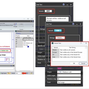


 Tim’s Takeaways: One for the Archives
 The Shaughnessy Report: All Together Now—The Value of Collaboration
 The Pulse: Overconstraining: Short, Slim, and Smooth
DFM 101: Final Finishes—OSP
March 9, 2023 | Anaya Vardya, American Standard CircuitsEstimated reading time: 1 minute

Introduction
One of the biggest challenges facing PCB designers is not understanding the cost drivers in the PCB manufacturing process. The next final finishes to discuss in this series is OSP. As with all surface finishes there are pros and cons with the decision of which to use. It is a combination of application, cost, and the properties of the finish. OSP is RoHS-compliant as there is zero lead content in the finish.
Final Finishes
OSP (Organic Solderability Preservative)
OSP is a thin organic coating, typically 5.9 to 11.8 µin [0.15 to 0.30 µm] thick, designed to prevent the oxidation of copper to maintain solderability over an extended period. Compared with other surface finish technologies, OSP is somewhat different. It uses a chemical process to produce an organic film on the bare copper surface which acts as a barrier to copper oxidation. OSP is organic, not metallic, and its cost is lower than most surface treatment technologies.
As with all surface finishes, the primary purpose is to protect the solderable surfaces on the PCB from oxidation and to aid in assembly soldering. This process coats a very thin coating of an organic material that inhibits copper oxidation. It is so thin that it is nearly impossible to see and measure. The organic material is removed by the assembly flux. Boards that have been OSP coated will have bright copper pad coloration. OSP is specially designed for mixed metal applications, such as electroless nickel immersion gold (ENIG). The OSP selectively deposits on copper while leaving gold connectors or metallic heat sinks free of contamination.
There are a couple of common OSP finishes widely used in the industry:
ENTEK CU-56: This is used for assemblies that will only go through a single reflow process. This finish is not being utilized much anymore because of the use of mixed technology boards (SMT and through-hole).
ENTEK CU-106A: This is the most prevalent version primarily due to the ability to survive multiple thermal assembly operations. PCBs that have multiple surface finishes can use the CU-106A(X) finish.
To read this entire article, which appeared in the February 2023 issue of Design007 Magazine, click here.
Share on:


Suggested Items
The Pulse: Overconstraining: Short, Slim, and Smooth
06/06/2024 | Martyn Gaudion -- Column: The PulseEngineering is both an art and a science. The design engineer’s task is (almost) always to bring product to market that meets specifications at the best and most economical price suited to the appropriate end use requirements. From a PCB perspective, designers are faced with a bewildering and almost overwhelming choice of materials at their disposal.
Connect the Dots: Designing for Reality—The Physical Manufacturing Phases
05/30/2024 | Matt Stevenson -- Column: Connect the DotsDesigning for reality is focused on the art and science of PCB design and production. If you’re trying to make a PCB that stands out for being reliable, easy to manufacture, and meets all design goals, then you’re in the perfect spot. We’re here to break down the PCB manufacturing process while sharing essential tips for smooth design and production.
DuPont Showcases AI Innovations Featuring Advanced Interconnects at 2024 International Electronic Circuits Exhibition
05/13/2024 | DuPontDuPont announced it will showcase its comprehensive range of advanced circuit materials and solutions at the 2024 International Electronic Circuits Exhibition in Shanghai. With a product portfolio that includes fine line, signal integrity, power and thermal management, DuPont will exhibit at Booth #8L06 at the National Exhibition and Convention Center (NECC) from May 13 to 15.
MKS’ Atotech to Participate in ECTC
05/10/2024 | MKS’ AtotechAt this year’s 74th IEEE Electronic Components and Technology Conference (ECTC), MKS’ Atotech will present and demonstrate its latest product and service innovations.
The Chemical Connection: Reducing Etch System Water Usage, Part 2
05/02/2024 | Don Ball -- Column: The Chemical ConnectionIn my last column, I reviewed some relatively simple ways to reduce water usage in existing etch systems: cutting down cooling coil water flow, adding chillers to replace plant water for cooling, lowering flow rate nozzles for rinses, etc. This month, I’ll continue with more ways to control water usage in your etcher. Most of these are not easily retrofittable to existing equipment but should be given serious consideration when new equipment is contemplated. With the right combination of add-ons, it is possible to bring the amount of water used in an etch system to almost zero.