-

- News
- Books
Featured Books
- design007 Magazine
Latest Issues
Current Issue
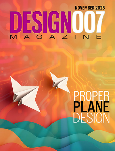
Designing Proper Work-Life Balance
In this issue, we hear from designers, marketers, and business owners on how they apply their professional skills to their personal lives to build a healthier work-life balance.

Designing Proper Planes
Without planes, designers would have to create thousands of traces to accomplish the same objectives. Power planes provide low impedance and stable power, and ground planes stabilize reference voltage, improve thermal performance, and help preclude EMI issues.

Power Integrity
Current power demands are increasing, especially with AI, 5G, and EV chips. This month, our experts share “watt’s up” with power integrity, from planning and layout through measurement and manufacturing.
- Articles
- Columns
- Links
- Media kit
||| MENU - design007 Magazine
Stitching Capacitor: Crosstalk Mitigation for Return Path Discontinuity
June 13, 2019 | Chang Fei Yee, Keysight TechnologiesEstimated reading time: 2 minutes
This article discusses the impact of stitching capacitors in mitigating signal crosstalk due to return path discontinuity during layer transition on PCB. The investigation was performed with 3DEM simulation using Keysight EMPro.
Introduction
In electronic systems, signal transmission exists in a close loop form. The forward current propagates from transmitter to receiver through the signal trace. On the contrary, the return current travels backward from receiver to transmitter through the power or ground plane right underneath the signal trace that serves as the reference or return path. The path of the forward current and return current forms a loop inductance. It is important to route the high-speed signal on a continuous reference plane so that the return current can propagate on the desired path, directly beneath the signal trace.
When the return path is broken due to the switching of reference planes with different potential, e.g., from ground to power or vice versa after layer transition on PCB, the return current might detour and propagate on a longer path, which causes a rise in loop inductance. This might lead to the sharing of a common return path by different signals that pose a high risk of interference among the signals due to higher mutual inductance. This interference results in signal crosstalk. To mitigate the crosstalk due to return path discontinuity (RPD), stitching capacitors are mounted on the PCB to serve as a bridge between the two reference planes of interest on different PCB layers.
Analysis of Signal Crosstalk
To investigate the impact of stitching capacitor in mitigating signal crosstalk due to RPD during layer transition on PCB, three simulation models of 3DEM are constructed. In model 1A (Figure 1), two signal traces with 50 ohm characteristic impedance in single-ended mode on the top PCB layer transition to the bottom layer using vias. Each segment of the signal traces on top and bottom layers is 100 mil long and 5 mil wide. Meanwhile, the diameters of the via barrel and pad are 5 mil and 7 mil respectively. The PCB stackup shown in Figure 2 is applied to this 3D model, where solid planes exist on layer 2 and 3. All the four copper layers are 1.2 mil thick and FR-4 material is used as the PCB substrate.
The two signal traces are 15 mil apart, which is triple the signal trace width for minimum crosstalk due to forward current propagation. A stitching via is placed 20 mil off each signal via, connected to the reference plane on layer 2 and extending to layer 4. However, voids are placed on the layer 3 reference plane to break the electrical connectivity between the planes on layer 2 and 3. This simulates the effect of RPD on signal crosstalk by switching the reference from ground to power or vice versa after the signal layer transition through the via.
To read this entire article, which appeared in the June 2019 issue of Design007 Magazine, click here.
Testimonial
"Your magazines are a great platform for people to exchange knowledge. Thank you for the work that you do."
Simon Khesin - Schmoll MaschinenSuggested Items
Elephantech Unveils HDI Microvia Formation Process Using Copper Nanoparticle Ink
12/29/2025 | ElephantechJapanese deep-tech Elephantech announced successful development of an innovative process to form High-Density Interconnect (HDI) microvia leveraging the company’s copper nanoparticle ink, named “Cu Nano Direct Plating.”
TopLine Introduces Cost-Efficient Flip Chips with Daisy Chain for Electrical Test Learning
12/23/2025 | TopLine CorporationFlip Chips with Daisy Chain from TopLine Corporation are a cost-efficient way to learn electrical test for engineers seeking to understand and practice necessary techniques for working with Flip Chip components.
Elephantech Launches Copper-on-Copper Self-Assembled Nanoparticles
12/22/2025 | ElephantechJapanese deep-tech startup Elephantech Inc. announced the successful development of Self-Assembled Copper Nanoparticles (SA-CuNP), a breakthrough technology that imparts dispersibility to copper microparticle pastes through an entirely new mechanism.
Connect the Dots: The Future of Designing for Reality—Outer Layer Imaging
12/24/2025 | Matt Stevenson -- Column: Connect the DotsIf you read my column regularly, you know I’m passionate about helping designers get the most from their designs. In my November column, I focused on designer best practices for the electroless copper component of the manufacturing process. The next step is outer layer imaging: the transition from digital to physical, and where the designer’s IP meets the board.
The Next Five Years of Thermal Substrates, Ceramics, and Thick-film PCBs
12/11/2025 | Brian Buyea, RemtecIf you want a clean view of where thermal substrates and ceramic/thick-film electronics are headed, follow the heat. Power density is moving up and to the right across industries: EV traction inverters, fast chargers, AI data centers, radar, satellite payloads, medical imaging, and high-brightness LEDs. The next five years will be defined by designs that treat thermal performance as a first-order constraint, not an afterthought. Here’s what that means in practice.


