


 Global PCB Connections: Rigid-flex and Flexible PCBs—The Backbone of Modern Electronics
 Flexible Thinking: The Key to a Successful Flex Circuit Design Transfer
 Happy’s Tech Talk #29: Bend-to-Install Semi-flex FR-4


Development of Flexible Hybrid Electronics
August 14, 2019 | Weifeng Liu, PhD, FlexEstimated reading time: 1 minute
Introduction
Flexible hybrid electronics (FHE) refers to a category of flexible electronics that are made through a combination of traditional assembly process of electronic components with high-precision ink printing technologies . By integrating silicon components with printed inks and flexible substrates, FHE will revolutionize the IoT and wearable industries. With FHE, designers can create a heterogeneous electronic system that can be fully integrated with different sensors, lighter in weight, more cost effective, more flexible and conforming to the curves of a human body or even stretchable across the shape of an object or structure—all while preserving the full functionality of traditional electronic systems.
The FHE industry is still in the early stages of development, and a variety of design, material, assembly and reliability issues need to be addressed. For example, electrical interconnections formed with conductive adhesives may not be as conductive or reliable as compared to conventional solder assembly. Typical polymer-based conductive inks are not as conductive as the etched copper used to make circuit boards and they are mostly not readily solderable. Additionally, commercially available stretchable thermoplastic-based film substrates have relatively low heat resistance and cannot withstand the current lead-free reflow process temperatures.
This article will present a hybrid manufacturing process to manufacture FHE systems with a two-layer interconnect structure utilizing screen printing of silver conductive ink, filled microvias to connect ink traces at the different layers, and use of the traditional reflow process to attach the semiconductor chips to the printed substrates.
Experimental
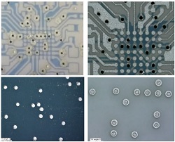
This study is to convert a rigid multilayer wearable development platform into a flexible one using printed conductive ink and flexible substrate. The current rigid platform contains two active semiconductor components and dozens of passive devices. The largest component is the microprocessor chip. Figure 1 shows the footprint for the microprocessor chip. It is an LGA package with 8X8 array and 64 I/Os. The pad size is 250 mm and the pitch is 400 mm, which leaves the space between pads at 150 mm.
To read this entire article, which appeared in the July 2019 issue of Design007 Magazine, click here.
Share on:


Testimonial
"In a year when every marketing dollar mattered, I chose to keep I-Connect007 in our 2025 plan. Their commitment to high-quality, insightful content aligns with Koh Young’s values and helps readers navigate a changing industry. "
Brent Fischthal - Koh YoungSuggested Items
Indium Experts to Deliver Technical Presentations at SMTA International
10/14/2025 | Indium CorporationAs one of the leading materials providers to the power electronics assembly industry, Indium Corporation experts will share their technical insight on a wide range of innovative solder solutions at SMTA International (SMTAI), to be held October 19-23 in Rosemont, Illinois.
Knocking Down the Bone Pile: Revamp Your Components with BGA Reballing
10/14/2025 | Nash Bell -- Column: Knocking Down the Bone PileBall grid array (BGA) components evolved from pin grid array (PGA) devices, carrying over many of the same electrical benefits while introducing a more compact and efficient interconnect format. Instead of discrete leads, BGAs rely on solder balls on the underside of the package to connect to the PCB. In some advanced designs, solder balls are on both the PCB and the BGA package. In stacked configurations, such as package-on-package (PoP), these solder balls also interconnect multiple packages, enabling higher functionality in a smaller footprint.
Indium to Showcase High-Reliability Solder and Flux-Cored Wire Solutions at SMTA International
10/09/2025 | Indium CorporationAs one of the leading materials providers in the electronics industry, Indium Corporation® will feature its innovative, high-reliability solder and flux-cored wire products at SMTA International (SMTAI), to be held October 19-23 in Rosemont, Illinois.
‘Create your Connections’ – Rehm at productronica 2025 in Munich
10/08/2025 | Rehm Thermal SystemsThe electronics industry is undergoing dynamic transformation: smart production lines, sustainability, artificial intelligence, and sensor technologies dominate current discussions.
Amplifying Innovation: New Podcast Series Spotlights Electronics Industry Leaders
10/08/2025 | I-Connect007In the debut episode, “Building Reliability: KOKI’s Approach to Solder Joint Challenges,” host Marcy LaRont speaks with Shantanu Joshi, Head of Customer Solutions and Operational Excellence at KOKI Solder America. They explore how advanced materials, such as crack-free fluxes and zero-flux-residue solder pastes, are addressing issues like voiding, heat dissipation, and solder joint reliability in demanding applications, where failure can result in costly repairs or even catastrophic loss.