


 It’s Only Common Sense: Your Biggest Competitor Is Complacency
 The Chemical Connection: Onshoring PCB Production—Daunting but Certainly Possible


Decreasing Bend Radius and Improving Reliability—Part I
October 11, 2019 | Kelsey Smith, All FlexEstimated reading time: 1 minute
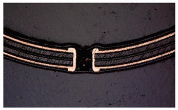
Application: Design guidelines to improve the flexibility and reliability of flexible circuits.
Many of the issues that arise when using a flex circuit come from a lack of knowledge about how to properly design one, especially when the circuit is required to bend. Many novices will design a circuit that calls for bending the flex in too tight of a bend radius, which can cause damage to the circuit and lower the reliability of the end product. This series of articles will focus on the seven key aspects to consider when designing for maximum durability and maximum “flexibility.” It is important to know that because flexibility is a relative term, this study will instead use the phrase "reducing bend radius." Here are two of the seven design strategies (please see Part II and Part III for more tips):
1. Reduce overall thickness:
IPC guidelines typically list minimum bend radius of 6X the circuit thickness for single-sided flex, 10X for double-sided flex, and 20X for multiple layer flex. The area of focus is the thickness where flexing or bending will occur, which should be only in a location with conductors and not plated through-holes. Thickness can best be reduced by:
A. Using thinner copper
B. Using adhesive-less base materials
C. Stagger conductors
D. Specifying button plating or pads only plating
Any flex circuit with plated through-holes will need to be either panel plated or button plated. Button plating is preferred because it only plates the vias and leaves the conductors un-plated and which does not increase the thickness.
2. Use only rolled annealed (RA) copper:
There are two common types of copper; rolled annealed (RA) and electro-deposited (ED) copper.
A. Rolled annealed copper is best for achieving a tighter bend radius.
B. It is also important for you to put on your drawings the direction of the grain in relation to where the tight bending will occur.
Go to Part two of this article.
Share on:


Testimonial
"Advertising in PCB007 Magazine has been a great way to showcase our bare board testers to the right audience. The I-Connect007 team makes the process smooth and professional. We’re proud to be featured in such a trusted publication."
Klaus Koziol - atgSuggested Items
Episode 6 of Ultra HDI Podcast Series Explores Copper-filled Microvias in Advanced PCB Design and Fabrication
10/15/2025 | I-Connect007I-Connect007 has released Episode 6 of its acclaimed On the Line with... American Standard Circuits: Ultra High Density Interconnect (UHDI) podcast series. In this episode, “Copper Filling of Vias,” host Nolan Johnson once again welcomes John Johnson, Director of Quality and Advanced Technology at American Standard Circuits, for a deep dive into the pros and cons of copper plating microvias—from both the fabricator’s and designer’s perspectives.
Nolan’s Notes: Tariffs, Technologies, and Optimization
10/01/2025 | Nolan Johnson -- Column: Nolan's NotesLast month, SMT007 Magazine spotlighted India, and boy, did we pick a good time to do so. Tariff and trade news involving India was breaking like a storm surge. The U.S. tariffs shifted India from one of the most favorable trade agreements to the least favorable. Electronics continue to be exempt for the time being, but lest you think that we’re free and clear because we manufacture electronics, steel and aluminum are specifically called out at the 50% tariff levels.
MacDermid Alpha & Graphic PLC Lead UK’s First Horizontal Electroless Copper Installation
09/30/2025 | MacDermid Alpha & Graphic PLCMacDermid Alpha Electronics Solutions, a leading supplier of integrated materials and chemistries to the electronics industry, is proud to support Graphic PLC, a Somacis company, with the installation of the first horizontal electroless copper metallization process in the UK.
Electrodeposited Copper Foils Market to Grow by $11.7 Billion Over 2025-2032
09/18/2025 | Globe NewswireThe global electrodeposited copper foils market is poised for dynamic growth, driven by the rising adoption in advanced electronics and renewable energy storage solutions.
MacDermid Alpha Showcases Advanced Interconnect Solutions at PCIM Asia 2025
09/18/2025 | MacDermid Alpha Electronics SolutionsMacDermid Alpha Electronic Solutions, a global leader in materials for power electronics and semiconductor assembly, will showcase its latest interconnect innovations in electronic interconnect materials at PCIM Asia 2025, held from September 24 to 26 at the Shanghai New International Expo Centre, Booth N5-E30