


 American Made Advocacy: Rebuilding America’s Military Stockpiles Begins With Microelectronics
 The Right Approach: The End of an Era—DoD Proposes MIL-PRF-31032 Cancellation
 Defense Speak Interpreted: Hypersonics Report Back After Six Years of Silence


NASA Replans CLPS Delivery of VIPER to 2024 to Reduce Risk
July 18, 2022 | NASAEstimated reading time: 2 minutes
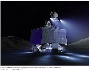
NASA’s Commercial Lunar Payload Services (CLPS) initiative allows rapid acquisition of lunar delivery services from American companies for payloads that advance capabilities for science, exploration or commercial development of the Moon. Through CLPS, NASA contracted Astrobotic of Pittsburgh to deliver the agency’s Volatiles Investigating Polar Exploration Rover (VIPER) to the lunar surface in search of ice and other potential resources. The measurements returned by VIPER will provide insight into the origin and distribution of water on the Moon and help determine how the Moon’s resources could be harvested for future human space exploration. While VIPER was originally scheduled for lunar delivery by Astrobotic in November 2023, NASA has requested the Astrobotic and VIPER mission teams to adjust VIPER’s delivery to the Moon’s South Pole to November 2024.
NASA’s decision to pursue a 2024 delivery date results from the agency’s request to Astrobotic for additional ground testing of the company’s Griffin lunar lander, which will deliver VIPER to the lunar surface through CLPS. The additional tests aim to reduce the overall risk to VIPER’s delivery to the Moon. To complete the additional NASA-mandated tests of the Griffin lunar lander, an additional $67.8 million has been added to Astrobotic’s CLPS contract, which now totals $320.4 million.
“Through CLPS, NASA has tasked U.S. companies to perform a very challenging technological feat – to successfully land and operate on the Moon,” said Joel Kearns, deputy associate administrator for exploration in NASA's Science Mission Directorate in Washington. “VIPER is NASA’s largest and most sophisticated science payload to be delivered to the Moon through CLPS, and we've implemented enhanced lander testing for this particular CLPS surface delivery.”
CLPS is a key part of NASA’s Artemis lunar exploration plans. The science and technology payloads sent to the Moon’s surface will help lay the foundation for human missions on and around the Moon. The agency has made seven task order awards to CLPS providers for lunar deliveries between in the early 2020s with more delivery awards expected through 2028.
Share on:


Testimonial
"We’re proud to call I-Connect007 a trusted partner. Their innovative approach and industry insight made our podcast collaboration a success by connecting us with the right audience and delivering real results."
Julia McCaffrey - NCAB GroupSuggested Items
Connect the Dots: Designing for the Future of Manufacturing Reality—Surface Finish
05/07/2026 | Matt Stevenson -- Column: Connect the DotsWhen designing the complex boards that many electronic devices require to operate, designers should consider manufacturability at every step. This is my last article focused on designing for the always-evolving manufacturing reality. Choosing the right surface finish has always been important. If you are creating intricate designs with a wide variety of components, like for an ultra-high density interconnect (UHDI) board, surface finish is a critical last step.
Elsyca Acquires Hivelix to Strengthen Simulation Platform for Electrochemical Surface Engineering
04/03/2026 | ElsycaElsyca, a global pioneer in computer-aided engineering (CAE) simulation for electrochemical processes and surface finishing, announces the acquisition of Hivelix, a specialist in advanced surface treatment simulation with strong expertise in multiphysics modelling and AI-assisted process optimisation.
Connect the Dots: Designing for the Future of Manufacturing Reality—Solder Mask and Legend
04/09/2026 | Matt Stevenson -- Column: Connect the DotsPCBs seem to be getting more complex by the day, so it is important for designers to keep educating themselves about the realities of manufacturing increasingly intricate boards. Last month’s column highlighted design considerations for the strip-etch-strip process and how manufacturers approach that phase of production. Now that we have a functioning board, we must protect the PCB from environmental hazards and document the circuit components. This article will detail the solder mask and legend process and offer best practices for designers to ensure a high-quality result.
Take the Mic: Photo Chemical Systems: 50 Years Strong
04/03/2026 | Real Time with... APEX EXPOPhoto Chemical Systems is celebrating 50 years in the bare board PCB market. David Graves and Jason Averette discuss how they've expanded into assembly, leveraging strong relationships and a customer-centric approach to navigate supply chain challenges. With innovative solutions and future growth strategies, including AI integration and new market ventures, Photo Chemical Systems continues enduring success.
Bold Laser Automation Introduces Precision Laser Cleaning System for Advanced Manufacturing
03/27/2026 | PRNewswireBold Laser Automation, Inc. has introduced the LPCl1820UV Laser Precision Cleaning System, a Class 1, industrial laser platform engineered for high-precision surface cleaning and thin-film removal in demanding manufacturing environments.