


 The Right Approach: I Hear the Train A Comin'
 It’s Only Common Sense: OCCAM—the Time Is Now
 Marcy's Musings: The Growing Industry
Another Big Shrink: Tiling Chiplets into Next-Generation Microsystems
July 21, 2016 | DARPAEstimated reading time: 3 minutes
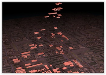
Open the hood of just about any electronic gadget and you probably will find printed circuit boards (PCBs)—most often in a leaf-green color—studded with processing, memory, data-relaying, graphics, and other types of chips and components, all interconnected with a labyrinth of finely embossed wiring. By challenging the technology community to integrate the collective functions hosted by an entire PCB onto a device approaching the size of a single chip, DARPA’s newest program is making a bid to usher in a fresh dimension of technology miniaturization.
“We are trying to push the massive amount of integration you typically get on a printed circuit board down into an even more compact format,” said Dr. Daniel Green, manager of the new program, whose acronym, “CHIPS,” is itself a typographic feat of miniaturization; the program’s full name is the Common Heterogeneous Integration and Intellectual Property (IP) Reuse Strategies Program. “It’s not just a fun acronym,” Green said. “The program is all about devising a physical library of component chips, or chiplets, that we can assemble in a modular fashion.”
A primary driver of CHIPS is to develop a novel, industry-friendly architectural strategy for designing and building new generations of microsystems in which the time and energy it takes to move signals—that is, data—between chips is reduced by factors of tens or even hundreds. “This is increasingly important for the data-intensive processing that we have to do as the data sets we are dealing with get bigger and bigger,” Green said. Although the program does not specify applications, the new architectural strategy at the program’s heart could open new routes to computational efficiencies required for such feats as identifying objects and actions in real-time video feeds, real-time language translation, and coordinating motion on-the-fly among swarms of fast-moving unmanned aerial vehicles (UAVs).
DARPA has posted a Request for Information (RFI), designated on fbo.gov as DARPA-SN-16-50, to harvest ideas at the front-end of the program from expert and industry players so that the CHIPS team can hone the details of the program in ways that would facilitate graceful incorporation of these new approaches within existing commercial semiconductor foundries and electronics fabrication facilities. “Key to the success of CHIPS will be standards and interfaces, and this means we will be working with a community, not all by ourselves,” said Green. The CHIPS team expects to use input from the RFI and a workshop anticipated to occur later this summer to prepare a Broad Agency Announcement (BAA). The BAA, which will also be posted on fbo.gov, will specify the program’s technical goals and how potential performers can submit proposals.
A major aspect of the CHIPS vision is the eventual availability of a library of custom and commercial “chiplets”—small-scale chips that individually embody a particular function, such as data storage, computation, signal processing, and managing the form and flow of data. By assembling and integrating dozens of chiplets, mosaic style, on a so-called interposer, which is like a printed circuit board writ small, all of those microsystems’ functions could be performed in a much closer huddle and can perform more efficiently than if they were distributed in the usual way among a suite of chips attached to a conventional PCB.
Another big win Green hopes to score with the modular architecture championed by the CHIPS program is the ability to separate out onto individual chiplets the many IP blocks developed for and aggregated into commercial monolithic chips. Such partitioning of computational functions could open the way for the DoD to negotiate more affordable licensing of smaller and more specific IP blocks suitable for repurposing for particular technologies and systems. “If CHIPS is successful, we will gain access to a wider variety of specialized IP blocks that we will be able to integrate into our systems more easily and with lower costs,” said Green. “This should be a win for both the commercial and defense sectors.”
Share on:


Suggested Items
KIC’s Miles Moreau to Present Profiling Basics and Best Practices at SMTA Wisconsin Chapter PCBA Profile Workshop
01/25/2024 | KICKIC, a renowned pioneer in thermal process and temperature measurement solutions for electronics manufacturing, announces that Miles Moreau, General Manager, will be a featured speaker at the SMTA Wisconsin Chapter In-Person PCBA Profile Workshop.
The Drive Toward UHDI and Substrates
09/20/2023 | I-Connect007 Editorial TeamPanasonic’s Darren Hitchcock spoke with the I-Connect007 Editorial Team on the complexities of moving toward ultra HDI manufacturing. As we learn in this conversation, the number of shifting constraints relative to traditional PCB fabrication is quite large and can sometimes conflict with each other.
Standard Of Excellence: The Products of the Future
09/19/2023 | Anaya Vardya -- Column: Standard of ExcellenceIn my last column, I discussed cutting-edge innovations in printed circuit board technology, focusing on innovative trends in ultra HDI, embedded passives and components, green PCBs, and advanced substrate materials. This month, I’m following up with the products these new PCB technologies are destined for. Why do we need all these new technologies?
Experience ViTrox's State-of-the-Art Offerings at SMTA Guadalajara 2023 Presented by Sales Channel Partner—SMTo Engineering
09/18/2023 | ViTroxViTrox, which aims to be the world’s most trusted technology company, is excited to announce that our trusted Sales Channel Partner (SCP) in Mexico, SMTo Engineering, S.A. de C.V., will be participating in SMTA Guadalajara Expo & Tech Forum. They will be exhibiting in Booth #911 from the 25th to the 26th of October 2023, at the Expo Guadalajara in Jalisco, Mexico.
Intel Unveils Industry-Leading Glass Substrates to Meet Demand for More Powerful Compute
09/18/2023 | IntelIntel announced one of the industry’s first glass substrates for next-generation advanced packaging, planned for the latter part of this decade.