ISBN: 978-1-959894-14-8
ISBN: 978-1-959894-17-9 Print-on-demand
 Anaya Vardya has over 40 years in the electronics manufacturing business and is currently the president and CEO of American Standard Circuits LLC. Anaya was previously COO of Canadian-based Coretec Inc. and senior VP of operations at Merix (both now part of TTM). He was also the corporate development manager at Continental Circuits, and before that, he held a variety of management and non-management positions in IBM Endicott and IBM Austin. Anaya holds a master’s degree in chemical engineering from the University of Cincinnati and a bachelor of technology from the Indian Institute of Technology.
About American Standard Circuits
In the world of DFM, American Standard Circuits and Sunstone Circuits come together as a unified PCB manufacturing powerhouse with over 50 years of combined experience. Together, they offer a comprehensive range of solutions and excel in producing ultra HDI, rigid, metal-backed, RF/microwave, flex, and rigid-flex PCBs for various industries, ranging from industrial to aerospace/defense.
This strategic alliance represents their dedication to delivering exceptional products and simplifying the PCB procurement process. By merging their strengths, they have set a groundbreaking standard in PCB manufacturing, providing engineers with the ultimate PCB solution for everything from design and prototypes to large-scale production, all based on the principles of Design for Manufacturability.
The company’s impressive certifications and advanced technology expertise reflect its commitment to excellence. They prioritize unparalleled customer support, ensuring that clients' needs are always met with precision and care.
 Kris Moyer Instructor, IPC
Kristopher Moyer is a distinguished PCB design expert with over 30 years of experience, boasting a portfolio of over 1000 PCB designs. With an educational background that includes an AS in electrical engineering from ITT Technical Institute and a BS in computer engineering from California State [...]
 Dana Korf Principal Consultant, Korf Consultancy LLC
Currently the principal consultant at Korf Consultancy LLC, Dana Korf works with companies to improve PCB fabricator front-end engineering processes. Dana is AME standards manager at Nano Dimension. He also works with OEMs and ODMs to create design rules and technology roadmaps, assist with supplier [...]
Chapter Summaries
-
Chapter 1
Materials
This chapter details high-frequency materials, copper foil types, metal core PCBs, and the benefits of embedded capacitance and resistor materials in multilayer PCBs.
-
Chapter 2
Panelization
Panelization outlines placing PCBs on manufacturing panels, highlighting features like coupons, borders, and scoring to maximize material utilization and reduce costs, and detailing preferred panel sizes and modifications.
-
Chapter 3
Controlled Impedance
Here, the author discusses controlled impedance PCB design, covering trace structures, impedance factors, modeling software, multiple impedance considerations, guidelines to minimize costs, and testing requirements.
-
Chapter 4
Material Construction Stackups
PCB stackup construction, guidelines for designing multilayer boards, balanced structure requirements, signal layer recommendations, and outer and internal layer guidelines are covered.
-
Chapter 5
Via Structures
The author explains the roles of through-holes and microvias in PCB design, detailing their types, uses, design considerations, and formation methods, such as mechanical and laser drilling.
-
Chapter 6
Plating Methods
Electroless and electroplating methods for PCBs, including pattern and panel plating, design compensation, surface-to-hole plating ratio, edge plating, and breakaway tabs for PCB arrays are explained here.
-
Chapter 7
Solder Mask and Legend
This chapter outlines PCB solder mask applications, including clearance requirements and via capping. It covers solder mask colors, legend marking with inkjet printers, and design constraints for legibility.
-
Chapter 8
Final Finishes and Design Guidelines
Various PCB final finishes, their applications, pros, cons, and design guidelines are explained. Key finishes include ENIG, ENEPIG, ENIPIG, ImmAg, ImmSn, HASL, and OSP, each with unique attributes.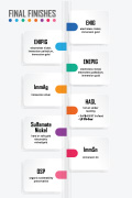
-
Chapter 9
Data Package Guidelines
Here, the reader will learn preferred and common data formats, requirements for drawing/data packages and array drawings, preferred artwork and drill data formats, and frequent critical and non-critical data issues in PCB fabrication.
-
Chapter 10
Cost Driver Summary
This chapter outlines cost drivers in PCB fabrication, highlighting factors like material costs, process complexities, density, and advanced technologies that impact overall cost.
Print-on-demand paperbacks are available for this title. Click below to order from our distributor.
What Our Readers Are Saying
The Companion Guide to DFM Essentials
Tips for Designing for Manufacturing is a comprehensive reference for PCB designers aiming to optimize their designs for manufacturability. It covers essential topics including preferred manufacturing data formats (like ODB++), fabrication notes, material specifications, layer stackups, controlled impedance, solder mask and surface finishes, and special requirements such as via fills and back-drilling. This guidebook also outlines common CAM issues and emphasizes early collaboration with fabricators to avoid costly design errors. Authored by American Standard Circuits and ASC Sunstone Circuits, readers will find this book reflects decades of expertise in delivering high- performance, reliable printed circuit boards.Inside, readers will find:


