
 It’s Only Common Sense: Make Your ‘Account’ the Whole Organization
 Dan’s Biz Bookshelf: ‘Building a Story Brand 2.0’
 Marcy’s Musings: A World of Difference





VSMC Celebrates the Grand Opening of Its First 300mm Fab in Singapore

VisionPower Semiconductor Manufacturing Company Pte. Ltd. (VSMC), the joint venture established in September 2024 by Vanguard International...
Indium Experts to Present Advanced Packaging, AI, and High-Performance Computing Materials Solutions at IMAPS Symposium

As a leading provider of high-reliability, AI-enabling soldering materials, three Indium Corporation experts will share new research and insights on...
ACCM Expands US Manufacturing Capacity for AI Infrastructure
Advanced Chip and Circuit Materials, Inc. (ACCM) announced a major expansion of its US manufacturing capacity for the Celeritas® family of advanced...
MKS Atotech Highlights Everplate Cu 300 2TF for Advanced Packaging
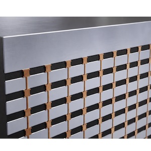
MKS Inc., a global provider of enabling technologies that transform our world, highlighted Everplate Cu 300 2TF from its Atotech...
Nordson Electronics Solutions to Showcase Dispensing and Plasma Systems at SEMICON West 2026
Nordson Electronics Solutions, a global leader in reliable electronics manufacturing technologies, will feature two new systems designed to address...
Asian Semiconductor Manufacturer Selects LPKF Glass Processing Equipment
LPKF Laser & Electronics SE has received a letter of Intent (LOI) for the purchase of NEXAR LIDE systems from a leading Asian advanced packaging...

Closing the Gap: Measuring 20-µm Spacing in Advanced SiP Packaging
September 18, 2026 | Axel Lindloff, Koh Young Europe

Twenty microns does not leave much room for error. As advanced packaging increases functional density, the distance between neighboring devices is shrinking to dimensions that create an entirely new set of inspection challenges. In some system-in-package (SiP) applications, components approximately 200 to 300 µm tall can be separated by gaps of only 20 to 30 µm. Measuring those spaces accurately requires considerably more than simply increasing camera magnification. The challenge is optical access.
Advanced Packaging and the New Scaling Walls
September 17, 2026 | Chetan Arvind Patil, Marvell Technology

Advanced packaging is becoming the foundation for semiconductor scaling in the AI era. As monolithic processors encounter practical limits around reticle size, yield, memory bandwidth, power, and cost, the industry is moving toward architectures built from multiple compute dies, HBM stacks, I/O chiplets, and heterogeneous packaging solutions. The result is that semiconductor scaling is no longer determined only by how much functionality can be integrated into a single die, but by how much silicon can be integrated efficiently within a package.





MORE ARTICLES
VSMC Celebrates the Grand Opening of Its First 300mm Fab in Singapore
September 28, 2026 | Globe Newswire
Indium Experts to Present Advanced Packaging, AI, and High-Performance Computing Materials Solutions at IMAPS Symposium
September 28, 2026 | Indium Corporation
ACCM Expands US Manufacturing Capacity for AI Infrastructure
September 28, 2026 | BUSINESS WIRE
MKS Atotech Highlights Everplate Cu 300 2TF for Advanced Packaging
September 28, 2026 | MKS Inc.
Nordson Electronics Solutions to Showcase Dispensing and Plasma Systems at SEMICON West 2026
September 25, 2026 | Nordson Electronics Solutions
Tata Electronics, Enomoto Sign MoU to Strengthen India Semiconductor Packaging
September 24, 2026 | Tata Electronics
Asian Semiconductor Manufacturer Selects LPKF Glass Processing Equipment
September 24, 2026 | LPKF
GSME, Teradyne Announce Strategic Partnership
September 23, 2026 | PRNewswire
Valens Semiconductor, onsemi Collaborate on Cost-Optimized MIPI A-PHY Sensor
September 23, 2026 | Valens Semiconductor
Qnity Joins PHLX Semiconductor Sector Index (SOX)
September 22, 2026 | BUSINESS WIRE
Testimonial
"The I-Connect007 team is outstanding—kind, responsive, and a true marketing partner. Their design team created fresh, eye-catching ads, and their editorial support polished our content to let our brand shine. Thank you all! "