


 It’s Only Common Sense: Being Your Customer’s Expert—The Key to Consultative Sales
 The Chemical Connection: Surface Finishes for PCBs
 The Marketing Minute: Go Big or Go Home—Long-form Content Is Your Brand’s Best Friend


200mm Fabs Thriving; SEMI’s Updated 200mm Fab Report Now Available
July 14, 2017 | SEMIEstimated reading time: 2 minutes
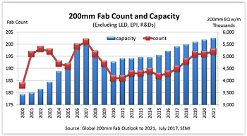
At SEMICON West in San Francisco, Calif., SEMI issued an update to its 200mm Fab Outlook report, with improved and expanded report forecasting of 200mm fab trends out to 2021. SEMI’s analysts updated information on over 100 facilities, including the latest new facilities and investment projects in China. The extensive new report "Global 200mm Fab Outlook to 2021" by SEMI tracks production, pilot, and R&D 200mm facilities worldwide with special attention on capacity expansions and new facilities.
Examining 200mm capacity over the years, the highest level of 200mm capacity was recorded in 2007 and the lowest following this peak in 2009. The capacity decline from 2007 to 2009 was driven by the 2008-2009 global financial crisis, which caused the closure of many facilities, and by the transition of memory and MPU fabrication to 300mm fabs from 200mm.
Since 2009, installed 200mm fab capacity has increased, and by 2020, 200mm capacity is expected to reach almost 5.7 million wafers per month (wpm), and poised to surpass the 2007 peak. According to SEMI’s World Fab Forecast data, by the end of this year, installed capacity will reach close to 5.4 million wpm.
Driven by mobile and wireless applications, IOT, and automotive, the 200mm market is thriving. Many of these products found their niche on 200mm wafers, so companies are expanding capacity in their facilities to the limit, and nine new 200mm facilities are in the pipeline. Looking only at IC volume fabs, the report shows 188 fabs in production in 2016 and expanding to 197 fabs by 2021.China will add most of the 200mm capacity through 2021 with 34 percent growth rate from 2017 to 2021, followed by South East Asia with 29 percent and the Americas with 12 percent.
The Global 200mm Fab Outlook to 2021, published by SEMI in July 2017, includes two files: a 92-page pdf file featuring trend charts, tables and summaries and an Excel file covering 2010 to 2021 detailing on quarterly basis and fab-by-fab developments. This is the third update since the report was first launched in 2015. Since the last report was published in November 2016, the SEMI analyst team has made 232 changes or updates to 132 fabs. The report tracks over 300 facilities using 200mm wafers from R&D, EPI, LED fabs to volume IC fabs.
About SEMI
SEMI connects nearly 2,000 member companies and 250,000 professionals worldwide annually to advance the technology and business of electronics manufacturing. SEMI members are responsible for the innovations in materials, design, equipment, software, and services that enable smarter, faster, more powerful, and more affordable electronic products. Since 1970, SEMI has built connections that have helped its members grow, create new markets, and address common industry challenges together. SEMI maintains offices in Bangalore, Beijing, Berlin, Brussels, Grenoble, Hsinchu, Seoul, Shanghai, Silicon Valley (Milpitas, Calif.), Singapore, Tokyo, and Washington, D.C.
Share on:


Suggested Items
Global Semiconductor Equipment Billings Surged to $117 Billion in 2024
04/10/2025 | SEMIWorldwide sales of semiconductor manufacturing equipment increased 10% to $117.1 billion in 2024 from $106.3 billion in 2023, SEMI, the industry association representing the global electronics design and manufacturing supply chain.
FTG Announces Q1 2025 Financial Results
04/10/2025 | Firan Technology Group CorporationIn Q1 2025, the Corporation grew through acquisition and organically. FTG is strategically investing its capital in ways that will drive increased shareholder returns for the future in both the near term and long term. The company's achievements in Q1 2025 demonstrate this commitment, laying a strong foundation for future growth.
Gartner Says Worldwide Semiconductor Revenue Grew 21% in 2024
04/10/2025 | Gartner, Inc.Worldwide semiconductor revenue totaled $655.9 billion in 2024, up 21% from $542.1 billion in 2023, according to final results by Gartner, Inc. NVIDIA climbed to the No. 1 position, overtaking Samsung Electronics and Intel for the first time.
Real Time With... IPC APEX EXPO 2025: Best Student Technical Paper Winner—Attila Rektor
04/10/2025 | Marcy LaRont, I-Connect007Attila Rektor, a Ph.D student from Boise State, won the best technical paper award at IPC APEX EXPO 2025. His paper explores enhancing the conductivity of laser-induced graphene for flexible circuits. The research, funded by SAIC, involved modulating surface energy to enable effective copper plating. This breakthrough has potential applications in flexible printed circuit boards, sensing, and biomedical devices.
IPC Hall of Fame Spotlight Series: Highlighting Walt Custer
04/09/2025 | Dan Feinberg, I-Connect007This Hall of Fame spotlight features a long-time associate of mine, Walt Custer. Now retired, Walt is well known in the industry for his decades of work as part of Custer Consulting Group, presenting his market research and business analyses at trade shows and conferences around the globe. As I mentioned in my spotlight on Gene Weiner, Walt and I were in that group that reported to Gene back in the old Dynachem days. Under Gene’s tutelage, we became deeply involved in IPC and were eventually honored with the Hall of Fame award.