


 Dan’s Biz Bookshelf: ‘Dream First, Details Later
 Happy’s Tech Talk #40: Factors in PTH Reliability—Hole Voids
 Facing the Future: Time for Real Talk, Early and Often, Between Design and Fabrication


Building Miniature Optical Antennas Using DNA as a Guide
February 5, 2018 | University of JyväskyläEstimated reading time: 2 minutes
A new fabrication technique combines programmable DNA origami shapes and conventional lithography methods to create metallic nanoantennas and chiral shapes for diverse applications.
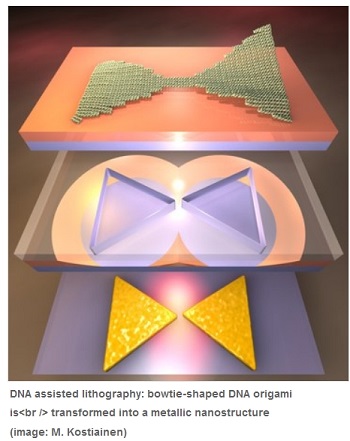
Research groups from University of Jyväskylä and Aalto University (Finland) together with researchers from California Institute of Technology (Caltech, USA) and Aarhus University (iNANO Center, Denmark) have reported a new highly parallel technique to fabricate precise metallic nanostructures with designed plasmonic properties by means of different self-assembled DNA origami shapes. The so-called DALI (DNA-assisted lithography) method has been published in the latest issue of Science Advances.
“We can build virtually any nanoscale shape using a DNA origami technique, and now we have shown how to use these accurate shapes as “stencils” to create millions of fully metallic nanostructures with 10 nm feature sizes in one go”, explains Adjunct Professor Veikko Linko from Aalto University. The trick in the DALI method is that when the DNA structures are deposited on a chip coated with silicon, silicon oxide can be selectively grown only on the bare areas of the substrate. “By controlling this process, we can create origami-shaped openings on the grown silicon oxide layer, and this layer can be used as a mask for the following lithography steps. Finally, we evaporate metal through these openings and create metallic structures having the same shape and size as the original DNA origami on a transparent substrate, such as sapphire”, Boxuan Shen from the Nanoscience Center of University of Jyväskylä describes the method.
The tiny metallic features cover the whole transparent substrate, and therefore these surfaces have intriguing optical properties. The small dimensions of the structures – in the range of ten nanometers – allow further tuning of these properties at the visible wavelength range. “Actually, we have demonstrated here a structure that we believe is the world’s smallest entirely metallic bowtie-shaped antenna. This extremely small size extends the operating range of optical features from infrared to visible”, states Adjunct Professor Jussi Toppari from Molecular Electronics and Plasmonics group at University of Jyväskylä. These antennas can find use in dozens of optical and plasmonic applications, such as surface enhanced Raman spectroscopy, biosensing or fluorescence enhancement. Moreover, the researchers demonstrated that the surfaces can be used as polarizers by fabricating chiral structures using DALI.
“The DALI method is highly parallel, and it could further enable cheap wafer-scale production of surfaces as it does not rely on costly patterning methods. It is also equipped for the future studies to provide bioinspired surfaces and metamaterials if the customized origami structures can be arranged on the substrate before metallization”, envisions Professor Mauri Kostiainen from the Biohybrid Materials Group at Aalto University.
Share on:


Suggested Items
The Chemical Connection: Through-glass Vias in Glass Substrates
06/24/2025 | Don Ball -- Column: The Chemical ConnectionThis month’s theme is vias and how best to ensure via quality and reliability. I don’t have much expertise in this process area or much to contribute that most of you don’t already know. However, I’ve recently become peripherally involved in a via technology that may be of more than academic interest to some of us. It entails putting vias in a material not usually associated with PCB manufacturing: through-glass vias (TGVs) in glass substrates.
Enough Talk—Time to Strengthen America’s Microelectronics Industrial Base
06/09/2025 | James Will, USPAEThe U.S. doesn’t have an innovation problem in terms of microelectronics, or a talent problem or even an investment problem. What the U.S. has is a coordination problem, and that’s threatening the livelihood of our domestic microelectronics ecosystem.
Ventec International Group Enters into a Fulfillment and Supply Agreement with Matrix and Launches Ventec Americas
06/09/2025 | Ventec International GroupVentec is excited to announce a new partnership with Matrix aimed at enhancing the fulfillment, value-added conversion, and distribution of PCB base materials across the North American market. This collaboration is set to significantly improve supply chain efficiency, and delivery performance for the company's North American customers.
AT&S Opens Europe’s First IC Substrate Plant and Competence Center in Leoben
06/04/2025 | AT&SAT&S officially inaugurated its new Competence Center for R&D and IC Substrate Production on Tuesday with a high-profile ceremony at its headquarters in Leoben-Hinterberg. Numerous high-ranking guests from politics, industry, and the media were welcomed to the event and given an exclusive tour of the 11,000-square-meter site of cutting-edge technology. With an investment of more than € 500 million,
IPC Applauds Leadership of Reps. Moore and Krishnamoorthi on PCB Manufacturing Bill
05/28/2025 | IPCIPC, the global electronics association serving more than 1,400 U.S. companies and over 3,200 worldwide, strongly supports the bipartisan reintroduction on May 28 of the Protecting Circuit Boards and Substrates (PCBS) Act in the 119th Congress.