


 The Right Approach: I Hear the Train A Comin'
 It’s Only Common Sense: OCCAM—the Time Is Now
 Marcy's Musings: The Growing Industry
Photovoltaic Nanotubes
June 20, 2019 | University of TokyoEstimated reading time: 3 minutes
Physicists discovered a novel kind of nanotube that generates current in the presence of light. Devices such as optical sensors and infrared imaging chips are likely applications, which could be useful in fields such as automated transport and astronomy. In future, if the effect can be magnified and the technology scaled up, it could lead to high-efficiency solar power devices.
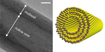
Image Caption: Transmission electron microscopy image of a hollow core nanotube. The white scale bar corresponds to 10 nanometers (left). Rendering of a nanotube (right).
Working with an international team of physicists, University of Tokyo Professor Yoshihiro Iwasa was exploring possible functions of a special semiconductor nanotube when he had a lightbulb moment. He took this proverbial lightbulb (which was in reality a laser) and shone it on the nanotube to discover something enlightening. Certain wavelengths and intensities of light induced a current in the sample — this is called the photovoltaic effect. There are several photovoltaic materials, but the nature and behavior of this nanotube is cause for excitement.
“Essentially our research material generates electricity like solar panels, but in a different way,” said Iwasa. “Together with Dr. Yijin Zhang from the Max Planck Institute for Solid State Research in Germany, we demonstrated for the first time nanomaterials could overcome an obstacle that will soon limit current solar technology. For now solar panels are as good as they can be, but our technology could improve upon that.”
The current-inducing nanotube is made from rolled-up sheets of a special semiconductor material based on tungsten disulfide (WS2). The sheets do not induce a current in the presence of light unless rolled into tubes. This is an emergent behavior, one not intrinsic to the material until it’s modified. What is interesting is how it differs from existing photovoltaic materials.
Generally, photovoltaic solar panels make use of a certain arrangement of materials called a p-n junction. This is where two different kinds of materials (p-type and n-type) are attached, which alone do not generate a current in the presence of light, but when placed together, do. P-n junction-based photovoltaics have improved in efficiency over the 80 years or so since their discovery. However, they are getting close to their theoretical limits due in part to their need for the arrangement of multiple materials.
WS2 nanotubes do not rely on a junction between materials to gain the photovoltaic effect. When exposed to light, they generate a current throughout their entire structure or bulk. This is called the bulk photovoltaic effect (BPVE) and it occurs as the WS2 nanotube is not symmetrical if you were to reverse it. If it were symmetrical, the current induced would not have a preferred direction and thus would not flow. So other symmetrical nanotubes — such as the famous carbon nanotubes — don't exhibit BPVE despite being great electrical conductors.
Four inset images. The lower right is a coarse grey texture. The other othree are orange geometric shapes on dark backgrounds.
Image Caption: Various iterations of the experimental nanotube device. Images captured by an atomic force microscope, and a scanning Kelvin probe microscope (lower right).
“Our research shows an entire order of magnitude improvement in efficiency of BPVE compared to its presence in other materials,” continued Iwasa. “But despite this huge gain, our WS2 nanotube cannot yet compare to the generating potential of p-n junction materials. This is because the device is nanoscopic and will be difficult to make larger. But it is possible and I hope chemists are inspired to take on that challenge.”
In the long term, researchers hope this kind of material could allow fabrication of more efficient solar panels. But given the foreseeable size constraints in the near term, it’s more likely to find use in other applications. BVPE could be used to create more sensitive and higher-fidelity optical or infrared sensors. These have further applications in embedded monitoring devices, sensor-laden self-driving cars or even in the imaging sensors for astronomical telescopes.
“My colleagues from around the world and I eagerly explore the potential of this unprecedented technology,” concluded Iwasa. “For me, the idea of creating new materials beyond anything nature could provide is a fascinating reward in its own right.”
Share on:


Suggested Items
Warm Windows and Streamlined Skin Patches – IDTechEx Explores Flexible and Printed Electronics
04/26/2024 | IDTechExFlexible and printed electronics can be integrated into cars and homes to create modern aesthetics that are beneficial and easy to use. From luminous car controls to food labels that communicate the quality of food, the uses of this technology are endless and can upgrade many areas of everyday life.
iNEMI Packaging Tech Topic Series: Role of EDA in Advanced Semiconductor Packaging
04/26/2024 | iNEMIAdvanced semiconductor packaging with heterogenous integration has made on-package integration of multiple chips a crucial part of finding alternatives to transistor scaling. Historically, EDA tools for front-end and back-end design have evolved separately; however, design complexity and the increased number of die-to-die or die-to-substrate interconnections has led to the need for EDA tools that can support integration of overall design planning, implementation, and system analysis in a single cockpit.
Koh Young Showcases Award-winning Inspection Solutions at SMTconnect with SmartRep in Hall 4A.225
04/25/2024 | Koh Young TechnologyKoh Young Technology, the industry leader in True 3D measurement-based inspection solutions, will showcase an array of award-winning inspection and measurement solutions at SMTconnect alongside its sales partner, SmartRep, in booth 4A.225 at NürnbergMesse from June 11-13, 2023. The following offers a glimpse into what Koh Young will present at the tradeshow:
Real Time with… IPC APEX EXPO 2024: Plasmatreat: Innovative Surface Preparation Solutions
04/25/2024 | Real Time with...IPC APEX EXPOIn this interview, Editor Nolan Johnson speaks with Hardev Grewal, CEO and president of Plasmatreat, a developer of atmospheric plasma solutions. Plasmatreat uses clean compressed air and electricity to create plasma, offering environmentally friendly methods for surface preparation. Their technology measures plasma density for process optimization and can remove organic micro-contamination. Nolan and Hardev also discuss REDOX-Tool, a new technology for removing metal oxides.
Nanotechnology Market to Surpass $53.51 Billion by 2031
04/25/2024 | PRNewswireSkyQuest projects that the nanotechnology market will attain a value of USD 53.51 billion by 2031, with a CAGR of 36.4% over the forecast period (2024-2031).