


 The Right Approach: I Hear the Train A Comin'
 It’s Only Common Sense: OCCAM—the Time Is Now
 Marcy's Musings: The Growing Industry
3D Printable 2D Materials-based Inks Show Promise to Improve Energy Storage Devices
July 31, 2019 | University of ManchesterEstimated reading time: 2 minutes
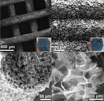
For the first time, a team of researchers, from the School of Materials and the National Graphene Institute at The the University of Manchester have formulated inks using the 2D material MXene, to produce 3D printed interdigitated electrodes.
MXene, a ‘clay-like’ two-dimensional material composed of early transition metals (such as titanium) and carbon atoms, was first developed by Drexel University. However, unlike most clays, MXene shows high electrical conductivity upon drying and is hydrophilic, allowing them to be easily dispersed in aqueous suspensions and inks.Since its isolation, graphene has opened the doors for the exploration of other two-dimensional materials, each with a range of different properties. However, in order to make use of these unique properties, 2D materials need to be efficiently integrated into devices and structures. The manufacturing approach and materials formulations are essential to realise this.
Dr Suelen Barg who led the team said: “We demonstrate that large MXene flakes spanning a few atoms thick, and water can be independently used to formulate inks with very specific viscoelastic behaviour for printing. These inks can be directly 3D printed into freestanding architectures over 20 layers tall. Due to the excellent electrical conductivity of MXene, we can employ our inks to directly 3D print current collector-free supercapacitors. The unique rheological properties combined with the sustainability of the approach open many opportunities to explore, especially in energy storage and applications requiring the functional properties of 2D MXene in customized 3D architectures.”
Wenji and Jae, PhD students at the Nano3D Lab at the University, said: “Additive manufacturing offers one possible method of building customised, multi-materials energy devices, demonstrating the capability to capture MXene’s potential for usage in energy applications. We hope this research will open avenues to fully unlock the potential of MXene for use in this field.”
The performance and application of these devices increasingly rely on the development and scalable manufacturing of innovative materials in order to enhance their performance.
Supercapacitors are devices that are able to produce massive amounts of power while using much less energy than conventional devices. There has been much work carried out on the use of 2D materials in these types of devices due to their excellent conductivity as well as having the potential to reduce the weight of the device.
Potential uses for these devices are for the automotive industry, such as in electric cars as well as for mobile phones and other electronics.
Share on:


Suggested Items
Designer’s Notebook: What Designers Need to Know About Manufacturing, Part 2
04/24/2024 | Vern Solberg -- Column: Designer's NotebookThe printed circuit board (PCB) is the primary base element for providing the interconnect platform for mounting and electrically joining electronic components. When assessing PCB design complexity, first consider the component area and board area ratio. If the surface area for the component interface is restricted, it may justify adopting multilayer or multilayer sequential buildup (SBU) PCB fabrication to enable a more efficient sub-surface circuit interconnect.
Insulectro’s 'Storekeepers' Extend Their Welcome to Technology Village at IPC APEX EXPO
04/03/2024 | InsulectroInsulectro, the largest distributor of materials for use in the manufacture of PCBs and printed electronics, welcomes attendees to its TECHNOLOGY VILLAGE during this year’s IPC APEX EXPO at the Anaheim Convention Center, April 9-11, 2024.
ENNOVI Introduces a New Flexible Circuit Production Process for Low Voltage Connectivity in EV Battery Cell Contacting Systems
04/03/2024 | PRNewswireENNOVI, a mobility electrification solutions partner, introduces a more advanced and sustainable way of producing flexible circuits for low voltage signals in electric vehicle (EV) battery cell contacting systems.
Heavy Copper PCBs: Bridging the Gap Between Design and Fabrication, Part 1
04/01/2024 | Yash Sutariya, Saturn Electronics ServicesThey call me Sparky. This is due to my talent for getting shocked by a variety of voltages and because I cannot seem to keep my hands out of power control cabinets. While I do not have the time to throw the knife switch to the off position, that doesn’t stop me from sticking screwdrivers into the fuse boxes. In all honesty, I’m lucky to be alive. Fortunately, I also have a talent for building high-voltage heavy copper circuit boards. Since this is where I spend most of my time, I can guide you through some potential design for manufacturability (DFM) hazards you may encounter with heavy copper design.
Trouble in Your Tank: Supporting IC Substrates and Advanced Packaging, Part 5
03/19/2024 | Michael Carano -- Column: Trouble in Your TankDirect metallization systems based on conductive graphite or carbon dispersion are quickly gaining acceptance worldwide. Indeed, the environmental and productivity gains one can achieve with these processes are outstanding. In today’s highly competitive and litigious environment, direct metallization reduces costs associated with compliance, waste treatment, and legal issues related to chemical exposure. What makes these processes leaders in the direct metallization space?