


 Driving Innovation: Mechanical and Optical Processes During Rigid-flex Production
 It’s Only Common Sense: Your Biggest Competitor Is Complacency
 The Chemical Connection: Onshoring PCB Production—Daunting but Certainly Possible


National Security in a Quantum World
August 9, 2019 | Imperial College LondonEstimated reading time: 3 minutes
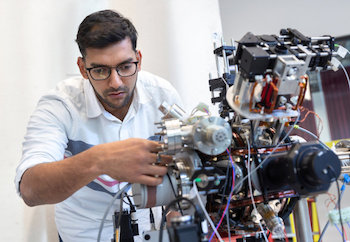
Imperial College London's security institute recently hosted an event on how quantum technology will impact national security. Advances in quantum technology, which applies quantum science in real-world applications, are poised to have a huge impact on national security.
At the ISST we recently hosted a briefing event with stakeholders from academia, industry and government to discuss some of the implications. Sir Peter Knight gave an overview of recent developments and what the future looks like, and Dr Indranil Dutta presented one particular application of quantum technology in more depth.
Quantum technology in national security
Quantum computing is probably the most widely discussed quantum technology, and whilst there have been massive strides made over the last decade or so, most predictions suggest we are still 10-15 years away from seeing this on a large-scale.
Quantum computers—whenever they do come—will pose a serious threat to the cryptographic systems which underpin much of our current computer security. Experts at the University of Waterloo have calculated that there is a 1 in 7 chance of these crypto primitives being affected by quantum attacks in 2026, and a 1 in 2 chance by 2031.
The message from Sir Peter Knight is that with so much data potentially at risk over the coming decade or so, the time to start thinking about this issue was last year.
Seeing Around Corners
There are many other applications of quantum theory in national security which are much closer to realisation however, which Sir Peter was particularly keen to highlight.
Quantum sensors is one such category with multiple use-cases on the horizon.
By taking advantage of the exquisite accuracy of quantum technology for measuring when a photon hits a sensor, you can develop sensing systems to visualise and track objects which are around corners, and out of the field of view.
One such system, developed by QuantIC in Glasgow, works by first shining a laser at the floor beyond the corner. As the light scatters off the floor, some will travel in the direction of and hit the objects around the corner. A tiny portion of this light will be reflected from the objects back to the floor, bouncing off in the direction of a sensor.
Ghost Imaging
Ghost imaging is another quantum technology which allows the visualisation of objects outside of the field of view. This relies on the slightly mind-boggling concept of quantum entanglement to build an image from photons which never interact with the object being imaged.
Light is passed through a carefully chosen crystal with the right nonlinear optical properties which will split some of the photons into two ‘entangled’ daughter photons. One of the daughter photons is directed towards the object to be imaged, and the other is directed towards the sensor doing the imaging.
The entangled photons have quantum states which are intrinsically linked and measurable, allowing the properties of the daughter that hits the object to be deducted from the other daughter that hits the sensor, ultimately allowing an image to be constructed.
The military and security applications for these imaging technologies are quite obvious, but they can also be applied to driverless cars and emergency rescue, to name only a couple of examples.
Quantum Navigation
Quantum sensing can also be used for navigation, as Dr Indranil Dutta, Senior Postdoctoral Researcher at Imperial College London, showed us.
Most navigation relies on Global Navigation Satellite Systems such as GPS. However, these can be locally jammed by inexpensive equipment, can be blocked by large structures, and can suffer global blackouts as shown by the recent malfunction in the EU’s Galileo system.
Indranil is part of a team developing a device which measures inertia to plot changes in a navigation path. It is much like an accelerometer, however current accelerometers which are found in mobile phones for example require an external reference to maintain accuracy over a long distance.
The quantum accelerometer does not rely on external signals and therefore cannot be jammed or blocked.
The device has a vacuum chamber, roughly the size of a watermelon, in which they hold and drop ultra-cold atoms whilst shining lasers at them as they fall through the chamber.
Because of their ultra-low temperature the atoms behave in a quantum way, as both a particle and a wave. If the device is moving, the acceleration will change the wave properties, which can be measured using the lasers.
At the end of 2018 the team demonstrated the device in a live event, and they are soon moving to test it in the real-world using shipping as the first use case.
The project is in collaboration with laser company M Squared, and funded by the Defence Science and Technology Laboratory, the Engineering and Physical Sciences Research Council, and Innovate UK.
Share on:


Testimonial
"Advertising in PCB007 Magazine has been a great way to showcase our bare board testers to the right audience. The I-Connect007 team makes the process smooth and professional. We’re proud to be featured in such a trusted publication."
Klaus Koziol - atgSuggested Items
Nvidia’s Blackwell Chips Made in Arizona Still Head to Taiwan for Final Assembly
10/27/2025 | I-Connect007 Editorial TeamNvidia has begun production of its next-generation Blackwell GPUs in the United States, but the company still depends heavily on Taiwan to complete the process, The Register reported.
American Standard Circuits Launches 50th 77-Second Webinar
10/27/2025 | American Standard CircuitsAnaya Vardya, President and CEO of American Standard Circuits/ASC Sunstone Circuits is pleased to announce that they have recently unveiled their 50th 77-second webinar.
KYZEN Brings Reliability to Life at productronica 2025 with ANALYST² Process Control Demos
10/22/2025 | KYZEN'KYZEN, the global leader in innovative environmentally responsible cleaning chemistries, will exhibit at productronica 2025, November 18–21 in Munich, Germany, where the company will put a spotlight on its award-winning KYZEN ANALYST² process control system in Hall A4, Stand 450.
SCHMID Group Secures Major Orders for AI Server PCB Production Equipment
10/22/2025 | SCHMID GroupSCHMID Group, a global equipment maker and solution provider for Printed Circuit Boards (PCB) and IC-Substrate manufacturing – announced the successful acquisition of two significant orders in the fast-growing field of PCB for artificial intelligence (AI) server applications. So called AI-Server-Boards.
SEMICON Japan 2025 to Spotlight Sustainability in AI and Semiconductor Innovation
10/22/2025 | SEMISEMICON Japan 2025, the largest gathering of leaders from the microelectronics manufacturing supply chain in Japan, will bring together more than 1,200 exhibitors showcasing semiconductor solutions from December 17-19 at Tokyo Big Sight.