


 Target Condition: Distribution of Power—Denounce the Ounce
 Fresh PCB Concepts: Resilience and Renewal in Domestic PCB Manufacturing
 Designers Notebook: Power and Ground Distribution Basics


Development of Flexible Hybrid Electronics
August 14, 2019 | Weifeng Liu, PhD, FlexEstimated reading time: 1 minute
Introduction
Flexible hybrid electronics (FHE) refers to a category of flexible electronics that are made through a combination of traditional assembly process of electronic components with high-precision ink printing technologies . By integrating silicon components with printed inks and flexible substrates, FHE will revolutionize the IoT and wearable industries. With FHE, designers can create a heterogeneous electronic system that can be fully integrated with different sensors, lighter in weight, more cost effective, more flexible and conforming to the curves of a human body or even stretchable across the shape of an object or structure—all while preserving the full functionality of traditional electronic systems.
The FHE industry is still in the early stages of development, and a variety of design, material, assembly and reliability issues need to be addressed. For example, electrical interconnections formed with conductive adhesives may not be as conductive or reliable as compared to conventional solder assembly. Typical polymer-based conductive inks are not as conductive as the etched copper used to make circuit boards and they are mostly not readily solderable. Additionally, commercially available stretchable thermoplastic-based film substrates have relatively low heat resistance and cannot withstand the current lead-free reflow process temperatures.
This article will present a hybrid manufacturing process to manufacture FHE systems with a two-layer interconnect structure utilizing screen printing of silver conductive ink, filled microvias to connect ink traces at the different layers, and use of the traditional reflow process to attach the semiconductor chips to the printed substrates.
Experimental
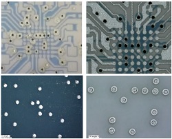
This study is to convert a rigid multilayer wearable development platform into a flexible one using printed conductive ink and flexible substrate. The current rigid platform contains two active semiconductor components and dozens of passive devices. The largest component is the microprocessor chip. Figure 1 shows the footprint for the microprocessor chip. It is an LGA package with 8X8 array and 64 I/Os. The pad size is 250 mm and the pitch is 400 mm, which leaves the space between pads at 150 mm.
To read this entire article, which appeared in the July 2019 issue of Design007 Magazine, click here.
Share on:


Testimonial
"In a year when every marketing dollar mattered, I chose to keep I-Connect007 in our 2025 plan. Their commitment to high-quality, insightful content aligns with Koh Young’s values and helps readers navigate a changing industry. "
Brent Fischthal - Koh YoungSuggested Items
Learning With Leo: UHDI—The Next Leap in PCB Manufacturing
11/05/2025 | Leo Lambert -- Column: Learning With LeoHigh density interconnect (HDI) technology has been a cornerstone of miniaturized electronics since Hewlett-Packard introduced the first chip-scale implementation in 1982. Over time, HDI processes became central to organic flip-chip packaging in the semiconductor industry. Today, the convergence of IC substrates and system-level PCBs has accelerated the adoption of UHDI.
BTU International Earns 2025 Step-by-Step Excellence Award for Its Aqua Scrub™ Flux Management System
10/29/2025 | BTU International, Inc.BTU International, Inc., a leading supplier of advanced thermal processing equipment for the electronics manufacturing market, has been recognized with a 2025 Step-by-Step Excellence Award (SbSEA) for its Aqua Scrub™ Flux Management Technology, featured on the company’s Pyramax™ and Aurora™ reflow ovens.
On the Line With… Ultra HDI Podcast—Episode 7: “Solder Mask: Beyond the Traces,” Now Available
10/31/2025 | I-Connect007I-Connect007 is excited to announce the release of the seventh episode of its 12-part podcast series, On the Line With… American Standard Circuits: Ultra HDI. In this episode, “Solder Mask: Beyond the Traces,” host Nolan Johnson sits down with John Johnson, Director of Quality and Advanced Technology at American Standard Circuits, to explore the essential role that solder mask plays in the Ultra HDI (UHDI) manufacturing process.
Rehm Wins Mexico Technology Award for CondensoXLine with Formic Acid
10/17/2025 | Rehm Thermal SystemsModern electronics manufacturing requires technologies with high reliability. By using formic acid in convection, condensation, and contact soldering, Rehm Thermal Systems’ equipment ensures reliable, void-free solder joints — even when using flux-free solder pastes.
Indium Experts to Deliver Technical Presentations at SMTA International
10/14/2025 | Indium CorporationAs one of the leading materials providers to the power electronics assembly industry, Indium Corporation experts will share their technical insight on a wide range of innovative solder solutions at SMTA International (SMTAI), to be held October 19-23 in Rosemont, Illinois.