


 Driving Innovation: Mechanical and Optical Processes During Rigid-flex Production
 It’s Only Common Sense: Your Biggest Competitor Is Complacency
 The Chemical Connection: Onshoring PCB Production—Daunting but Certainly Possible


Seeing Infrared: Sandia’s Nanoantennas Help Detectors See More Heat, Less Noise
September 17, 2019 | Sandia National LaboratoriesEstimated reading time: 3 minutes
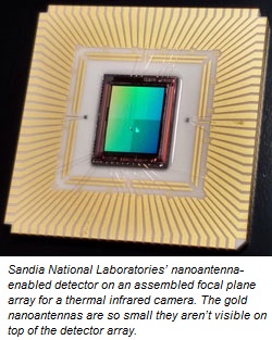
Sandia National Laboratories researchers have developed tiny, gold antennas to help cameras and sensors that “see” heat deliver clearer pictures of thermal infrared radiation for everything from stars and galaxies to people, buildings and items requiring security.
In a Laboratory Directed Research and Development project, a team of researchers developed a nanoantenna-enabled detector that can boost the signal of a thermal infrared camera by up to three times and improve image quality by reducing dark current, a major component of image noise, by 10 to 100 times.
Thermal infrared cameras and sensors have existed for 50 years, but the traditional design of the detector that sits behind the camera lens or a sensor’s optical system seems to be reaching its performance limits, said David Peters, a Sandia manager and nanoantenna project lead.
He said improved sensitivity in infrared detectors, beyond what the typical design can deliver, is important for both Sandia’s national security work and for other uses, such as astronomical research.
Seeing More with Less
The sensitivity and image quality of an infrared detector usually depends on a thick layer of detector material that absorbs incoming heat and turns it into an electrical signal that can be collected and turned into an image. The thickness of the detector layer determines how much heat can be absorbed and read by the camera, but thick layers also have drawbacks.
“The detector material is always spontaneously creating electrons that are collected and add noise to the image, which reduces image quality,” Peters said. “This phenomenon, called dark current, increases along with the thickness of the detector material — the thicker the material is, the more noise in the image it creates.”
The research team developed a new detector design that breaks away from relying on thick layers and instead uses a subwavelength nanoantenna, a patterned array of gold square or cross shapes, to concentrate the light on a thinner layer of detector material. This design uses just a fraction of a micron of detector material, whereas traditional thermal infrared detectors have a thickness of 5 to 10 microns. A human hair is about 75 microns in width.
The nanoantenna-enhanced design helps detectors see more than 50% of an object’s infrared radiation while also reducing image distortion caused by dark current, whereas current technology can only see about 25% of infrared radiation. It also allows for the invention of new detector concepts that are not possible with existing technology.
“For example, with nanoantennas, it’s possible to dramatically expand the amount of information acquired in an image by exquisitely controlling the spectral response at the pixel level,” Peters said.
The team makes the nanoantenna-enabled detectors by slightly altering the usual process for making an infrared detector. It starts by “growing” the detector material on top of a thin disk called a wafer. Then the detector material is flipped onto a layer of electronics that read the signals collected by the nanoantenna and the detector layer. After discarding the wafer, a tiny amount of gold is applied to create the patterned nanoantenna layer on top of the detector material.
From National Lab to Industry
“It was not a given that this was going to work, so that’s why Sandia took it on,” Peters said. “Now, we are to the point where we have proven this concept and this technology is ready to be commercialized. This concept can be applied to different detector types, so there’s an opportunity for existing manufacturers to integrate this new technology with their existing detectors.”
Peters said Sandia is pursuing leads to establish a Collaborative Research and Development Agreement to start transferring the technology to industry.
“This project is a perfect example of how a national lab can prove a concept and then spin it off to industry where it can be developed further,” Peters said.
This research was conducted at Sandia’s National Security Photonics Center. For more information about Sandia’s work in developing and delivering integrated photonics solutions for national security applications, visit the center’s website.
About Sandia National Laboratories
Sandia National Laboratories is a multimission laboratory operated by National Technology and Engineering Solutions of Sandia LLC, a wholly owned subsidiary of Honeywell International Inc., for the U.S. Department of Energy’s National Nuclear Security Administration. Sandia Labs has major research and development responsibilities in nuclear deterrence, global security, defense, energy technologies and economic competitiveness, with main facilities in Albuquerque, New Mexico, and Livermore, California.
Share on:


Testimonial
"Your magazines are a great platform for people to exchange knowledge. Thank you for the work that you do."
Simon Khesin - Schmoll MaschinenSuggested Items
Designers Notebook: Power and Ground Distribution Basics
10/29/2025 | Vern Solberg -- Column: Designer's NotebookThe principal objectives to be established during the planning stage are to define the interrelationship between all component elements and confirm that there is sufficient surface area for placement, the space needed to ensure efficient circuit interconnect, and to accommodate adequate power and ground distribution.
The Marketing Minute: Marketing With Layers
10/15/2025 | Brittany Martin -- Column: The Marketing MinuteMarketing to a technical audience is like crafting a multilayer board: Each layer serves a purpose, from the surface story to the buried detail that keeps everything connected. At I-Connect007, we’ve learned that the best marketing campaigns aren’t built linearly; they’re layered. A campaign might start with a highly technical resource, such as an in-depth article, a white paper, or a podcast featuring an engineer delving into the details of a process. That’s the foundation, the substance that earns credibility.
EDADOC Ushers in a New Era of Robotics Innovation
10/07/2025 | Edy Yu, Editor-in-Chief, ECIOOn Sept. 11, Shanghai Zhiyuan Technology Co., Ltd. (MScape) made a stunning debut at Shanghai’s 2025 Fourth North Bund Cybersecurity Forum and Cyber Intelligence Security Frontier Technology and Equipment Exhibition. The company presented the world’s first Dvorak super heterogeneous architecture and the Zhijing T-series-embodied intelligence (robotics) edge computing power platform. This has been a game-changer in the cybersecurity technology field, filling the gap in the domestic robotics core computing power platform.
Connect the Dots: Evolution of PCB Manufacturing—Lamination
10/02/2025 | Matt Stevenson -- Column: Connect the DotsWhen I wrote The Printed Circuit Designer's Guide to...™ Designing for Reality, it was not a one-and-done effort. Technology is advancing rapidly. Designing for the reality of PCB manufacturing will continue to evolve. That’s why I encourage designers to stay on top of the tools and processes used during production, to ensure their designs capitalize on the capabilities of their manufacturing partner.
Driving Innovation: Mastering Panel Warpage
09/23/2025 | Simon Khesin -- Column: Driving InnovationDuring the complex and multi-step process of PCB fabrication, a panel's flatness is constantly at risk. A host of factors can introduce warpage, bending, and unevenness, presenting a fundamental challenge to achieving high-precision results. This deformation (sometimes referred to as “bow and twist”), even on a microscopic scale, can lead to critical defects during subsequent stages, such as component surface mounting (e.g., tombstoning, solder opens) and the PCB's long-term functional reliability.