


 The Chemical Connection: Onshoring PCB Production—Daunting but Certainly Possible
 It’s Only Common Sense: The Phone Is Still Mightier Than the Keyboard


Moving E-Cars Into the Fast Lane
October 2, 2019 | Fraunhofer-GesellschaftEstimated reading time: 2 minutes
Researchers have been looking into silicon carbide, a promising alternative material for the semiconductor industry, for several years now. The Fraunhofer Institute for Reliability and Microintegration IZM joined forces with partners in the SiC Module project to ramp up this type of power semiconductor for industrial manufacturing. Their effort goes to boost the efficiency of drivetrains in electric vehicles and extend these vehicles’ range.
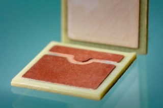
Embedded silicon carbide on its way to mass manufacturing for e-mobility applications.
Electromobility has its naysayers, with some skeptics pointing to limitations such as electric cars’ top speed and maximum range. Both depend on the built-in power electronics, the electronic heart of e-mobility. Size, weight and efficiency are three make-or-break factors for power electronics destined for installation in e-cars. Silicon carbide (SiC), a new semiconductor material, ticks all three boxes. It is more efficient yet leaves a smaller footprint than conventional semiconductors such as silicon.
Even so, silicon carbide is not to be found in any e-car on the road today. As it stands, this semiconductor material is still confined to research labs. To port it from the lab to the factory, the SiC Module project has factored all the conditions of industrial manufacturing into the equation from the outset. The module’s design is a case in point: Researchers at the Fraunhofer IZM are basing it on the structure of the classic printed circuit board that the industry has long favored. This should expedite its rollout.
Shorter power lines, better power routing
The module is also benefitting from the latest scientific advances. Rather than wire-bonding the semiconductor to the package, the researchers decided to embed it directly in the circuit with a galvanic-assisted copper contact to shorten the wires and optimize power routing. The team also brought the potential customer on board for this development effort. In the project’s first year, they drew up a specification sheet pinpointing the electrical, thermal and performance requirements for the module and semiconductor. The researchers worked closely with users, catering to their wishes when they determined the product specs. Automakers, component suppliers and OEMs were directly involved in the effort to map out the power-electronic modules’ size, layout and electrical circuits. This collective sought to make the most of the space available in the vehicles’ powertrain. Lars Böttcher, group leader at the Fraunhofer IZM and head of the SiC sub-project project, says, “We’re going beyond a general proof of concept because we are developing more than just a prototype in this project”. The goal is to ramp up both the new semiconductor material silicon carbide and the embedding technology for mass production.
The Federal Ministry of Education and Research is funding the project with 3.89 million euros as part of the E-Mobility Call. Slated to run from January 2018 to December 2020, the project involves six partners alongside the Fraunhofer IZM: AixControl – Gesellschaft für leistungselektronische Systemlösungen mbH, Conti Temic microelectronic GmbH, Rheinisch-Westfälischen Technischen Hochschule Aachen, Robert Bosch GmbH, Schweizer Electronic AG, and TLK-Thermo GmbH.
Share on:


Testimonial
"We’re proud to call I-Connect007 a trusted partner. Their innovative approach and industry insight made our podcast collaboration a success by connecting us with the right audience and delivering real results."
Julia McCaffrey - NCAB GroupSuggested Items
Episode 6 of Ultra HDI Podcast Series Explores Copper-filled Microvias in Advanced PCB Design and Fabrication
10/15/2025 | I-Connect007I-Connect007 has released Episode 6 of its acclaimed On the Line with... American Standard Circuits: Ultra High Density Interconnect (UHDI) podcast series. In this episode, “Copper Filling of Vias,” host Nolan Johnson once again welcomes John Johnson, Director of Quality and Advanced Technology at American Standard Circuits, for a deep dive into the pros and cons of copper plating microvias—from both the fabricator’s and designer’s perspectives.
Nolan’s Notes: Tariffs, Technologies, and Optimization
10/01/2025 | Nolan Johnson -- Column: Nolan's NotesLast month, SMT007 Magazine spotlighted India, and boy, did we pick a good time to do so. Tariff and trade news involving India was breaking like a storm surge. The U.S. tariffs shifted India from one of the most favorable trade agreements to the least favorable. Electronics continue to be exempt for the time being, but lest you think that we’re free and clear because we manufacture electronics, steel and aluminum are specifically called out at the 50% tariff levels.
MacDermid Alpha & Graphic PLC Lead UK’s First Horizontal Electroless Copper Installation
09/30/2025 | MacDermid Alpha & Graphic PLCMacDermid Alpha Electronics Solutions, a leading supplier of integrated materials and chemistries to the electronics industry, is proud to support Graphic PLC, a Somacis company, with the installation of the first horizontal electroless copper metallization process in the UK.
Electrodeposited Copper Foils Market to Grow by $11.7 Billion Over 2025-2032
09/18/2025 | Globe NewswireThe global electrodeposited copper foils market is poised for dynamic growth, driven by the rising adoption in advanced electronics and renewable energy storage solutions.
MacDermid Alpha Showcases Advanced Interconnect Solutions at PCIM Asia 2025
09/18/2025 | MacDermid Alpha Electronics SolutionsMacDermid Alpha Electronic Solutions, a global leader in materials for power electronics and semiconductor assembly, will showcase its latest interconnect innovations in electronic interconnect materials at PCIM Asia 2025, held from September 24 to 26 at the Shanghai New International Expo Centre, Booth N5-E30