


 It’s Only Common Sense: The Phone Is Still Mightier Than the Keyboard
 The Marketing Minute: Marketing With Layers


Space Saving, 3.3V I/O FBGA Two-Speed Synchro/Resolver Combiner from DDC
November 22, 2019 | Data Device Corporation (DDC)Estimated reading time: 1 minute
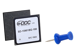
Data Device Corporation (DDC) introduces a redesigned version of its popular Synchro/Resolver two-speed combiner, now featuring 3.3V I/O within a compact and highly efficient FBGA (Fine Pitch Ball Grid Array) package. The SD-15901 FBGA design provides space and power savings with a 34% smaller footprint and 35% less power dissipation than the previous generation, enabling SWaP optimization of PCB layout and ease of assembly with ball grid array surface mounting.
Using coarse and fine digital angle inputs, the combiner provides up to 22-bit angle resolution, making it ideal for high-performance position control systems requiring real-time precision resolution. Additionally, the SD-15901 is RoHS compliant, and rated for the full military temperature range (-55°C to +125°C).
Benefits include:
- Optimized Performance and Design
- High resolution (up to 22 bits)
- Small footprint (23 mm x 23 mm) saves board space, 34% smaller compared with (28.4 mm x 28.4 mm) of previous generation
- Low power dissipation, 35% less power dissipated than previous generation (at nominal operation)
- FBGA design enables ease of assembly
- Flexibility & Ease of Use
- Can be used with all 3.3V Synchro/Resolver converters and processors, no logic shifters required
- No software or calibration required
- Environmental
- Military temperature range (-55°C to +125°C)
- RoHS compliant
"DDC’s second generation Synchro/Resolver two-speed combiner offers significant SWaP savings along with high resolution, to enable optimized PDB design," Roger Tomassi, DDC Product Line Manager, Motion Feedback.
Share on:


Testimonial
"In a year when every marketing dollar mattered, I chose to keep I-Connect007 in our 2025 plan. Their commitment to high-quality, insightful content aligns with Koh Young’s values and helps readers navigate a changing industry. "
Brent Fischthal - Koh YoungSuggested Items
Keysight Completes Acquisition of Synopsys’ Optical Solutions Group and Ansys’ PowerArtist
10/17/2025 | Keysight Technologies, Inc.Keysight Technologies, Inc., announced the completion of its acquisitions of the Optical Solutions Group from Synopsys, Inc., and PowerArtist from Ansys, Inc.
RT-Labs Joins STMicroelectronics Partner Program to Accelerate Industrial Communication
10/16/2025 | RT-LabsRT-Labs, a leading provider of real-time software solutions for industrial automation, announces that it has joined the STMicroelectronics Partner Program to integrate its Ethernet-based industrial communication stacks into ST’s development environments and microcontroller platforms.
ASC Sunstone Circuits Adds New Options to OneQuote While Maintaining Real-Time Pricing on Core PCB Features
10/16/2025 | ASC Sunstone CircuitsASC Sunstone Circuits, a leading U.S. PCB manufacturer, today announced a significant expansion of its OneQuote online quoting tool, giving design engineers more control over complex PCB configurations — making it easier for the quote team to quickly clarify and verify specifications, reducing delays from manual quote reviews.
Analog Devices Launches ADI Power Studio™ and New Web-Based Tools
10/14/2025 | Analog Devices, Inc.Analog Devices, Inc., a global semiconductor leader, announced the launch of ADI Power Studio, a comprehensive family of products that offers advanced modeling, component recommendations and efficiency analysis with simulation. In addition, ADI is introducing early versions of two new web-based tools with a modernized user experience under the Power Studio umbrella:
Cadence Giving Foundation Announces Multi-Year Commitment to Expand the AI Hub at San José State University
10/13/2025 | Cadence Design Systems, Inc.The Cadence Giving Foundation today announced a multi-year commitment to expand the AI Hub at San José State University (SJSU) to equip students with the skills, hands-on training and experience needed to excel in careers in artificial intelligence (AI).