


 The Chemical Connection: Onshoring PCB Production—Daunting but Certainly Possible
 It’s Only Common Sense: The Phone Is Still Mightier Than the Keyboard


Decreasing Bend Radius and Improving Reliability- Part II
November 22, 2019 | Kelsey Smith, All FlexEstimated reading time: 1 minute
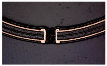
Application: Design guidelines to improve the flexibility and reliability of flexible circuits.
Many of the issues that arise when using a flex circuit come from a lack of knowledge about how to properly design one, especially when the circuit is required to bend. Many novices will design a circuit that calls for bending the flex in too tight of a bend radius, which can cause damage to the circuit and lower the reliability of the end product. This series of articles will focus on the seven key aspects to consider when designing for maximum durability and maximum “flexibility”. It is important to know that because flexibility is a relative term this study will instead use the term reducing bend radius. Below are two of the seven design strategies. Please see Part I and Part III for more tips!
3. Do not allow electroless copper as a seed layer prior to plating vias.
- Also, an area to be concerned about is the type of plating your vendor uses. Some copper plating requires a seed layer of electroless copper. This seed layer becomes an ED copper layer and can lead to conductor cracking. For a tight bend radius direct metallization is the preferred plating method.
4. Use only Polyimide covers in the flexing area.
- There are two options for applying dielectric material over copper:
A. Polyimide cover material: This is the preferred material in areas where parts will be bent. As a general rule, you will want to specify a dielectric thickness and adhesive thickness separately. A rule of thumb is that for every 1 ounce of copper thickness there is 1 mil of adhesive thickness.
B. Flexible Solder Mask: Flexible solder mask has a minimum bend radius of 0.4” and is not recommended for any dynamic flexing application or application where the bend radius will be tighter than 0.4”

Share on:


Testimonial
"We’re proud to call I-Connect007 a trusted partner. Their innovative approach and industry insight made our podcast collaboration a success by connecting us with the right audience and delivering real results."
Julia McCaffrey - NCAB GroupSuggested Items
Rehm Wins Mexico Technology Award for CondensoXLine with Formic Acid
10/17/2025 | Rehm Thermal SystemsModern electronics manufacturing requires technologies with high reliability. By using formic acid in convection, condensation, and contact soldering, Rehm Thermal Systems’ equipment ensures reliable, void-free solder joints — even when using flux-free solder pastes.
Indium Experts to Deliver Technical Presentations at SMTA International
10/14/2025 | Indium CorporationAs one of the leading materials providers to the power electronics assembly industry, Indium Corporation experts will share their technical insight on a wide range of innovative solder solutions at SMTA International (SMTAI), to be held October 19-23 in Rosemont, Illinois.
Knocking Down the Bone Pile: Revamp Your Components with BGA Reballing
10/14/2025 | Nash Bell -- Column: Knocking Down the Bone PileBall grid array (BGA) components evolved from pin grid array (PGA) devices, carrying over many of the same electrical benefits while introducing a more compact and efficient interconnect format. Instead of discrete leads, BGAs rely on solder balls on the underside of the package to connect to the PCB. In some advanced designs, solder balls are on both the PCB and the BGA package. In stacked configurations, such as package-on-package (PoP), these solder balls also interconnect multiple packages, enabling higher functionality in a smaller footprint.
Indium to Showcase High-Reliability Solder and Flux-Cored Wire Solutions at SMTA International
10/09/2025 | Indium CorporationAs one of the leading materials providers in the electronics industry, Indium Corporation® will feature its innovative, high-reliability solder and flux-cored wire products at SMTA International (SMTAI), to be held October 19-23 in Rosemont, Illinois.
‘Create your Connections’ – Rehm at productronica 2025 in Munich
10/08/2025 | Rehm Thermal SystemsThe electronics industry is undergoing dynamic transformation: smart production lines, sustainability, artificial intelligence, and sensor technologies dominate current discussions.
Copyright © I-Connect007 | IPC Publishing Group Inc. All rights reserved.
Log in