


 Facing the Future: The Role of 5G and Beyond in Shaping PCB Demand
 It’s Only Common Sense: Stop Pitching, Start Listening
 Trouble in Your Tank: Causes of Plating Voids, Pre-electroless Copper


EV Group Establishes Heterogeneous Integration Competence Center
March 3, 2020 | PR NewswireEstimated reading time: 2 minutes
EV Group (EVG), a leading supplier of wafer bonding and lithography equipment for the MEMS, nanotechnology and semiconductor markets, announced that it has established the Heterogeneous Integration Competence Center™, which is designed to assist customers in leveraging EVG's process solutions and expertise to enable new and enhanced products and applications driven by advances in system integration and packaging. These include solutions and applications for high-performance computing and data centers, the Internet of Things (IoT), autonomous vehicles, medical and wearable devices, photonics and advanced sensors.
The Heterogeneous Integration Competence Center™ combines EV Group’s world-class wafer bonding, thin-wafer handling, and lithography products and expertise, as well as pilot-line production facilities and services at its state-of-the-art cleanroom facilities.
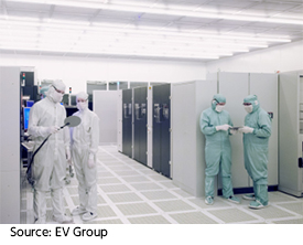
EVG’s HI Competence Center is designed to help enable new products and applications driven by advances in system integration and packaging. Shown here: chiplet integration by collective die-to-wafer hybrid bonding.
The Heterogeneous Integration (HI) Competence Center combines EVG's world-class wafer bonding, thin-wafer handling, and lithography products and expertise, as well as pilot-line production facilities and services at its state-of-the-art cleanroom facilities at EVG's headquarters in Austria, supported by EVG's worldwide network of process technology teams. Through the HI Competence Center, EVG will help customers to accelerate technology development, minimize risk, and develop differentiating technologies and products through heterogeneous integration and advanced packaging all while guaranteeing the highest IP protection standards that are required for working on pre-release products.
"Heterogeneous integration fuels new packaging architectures and demands new manufacturing technologies to support greater system and design flexibility, as well as increased performance and lower system design costs," stated Markus Wimplinger, corporate technology development & IP director of EV Group. "EVG's new HI Competence Center provides an open access innovation incubator for our customers and partners across the microelectronics supply chain to collaborate while pooling our solutions and process technology resources to shorten development cycles and time to market for innovative devices and applications enabled by heterogeneous integration."
EVG has an extensive background in heterogeneous integration, providing solutions for this key technology trend for more than 20 years. Among these are: permanent wafer bonding—including direct fusion and hybrid bonding for 3D packaging and metal bonding—and die-to-wafer bonding with and without collective carriers for integration of III-V compound semiconductors and silicon as well as high-density 3D packaging; temporary bonding and debonding, including mechanical, slide-off/lift-off, and UV laser assisted; thin-wafer handling; and innovative lithography technologies, including mask aligners, coaters and developers, and maskless exposure/digital lithography.
Advanced Packaging Milestones
In the field of permanent bonding, EVG pioneered the patented SmartView® wafer-to-wafer alignment system more than 20 years ago, and has refined this technology over the years to support breakthrough technology advances such as backside-illuminated CMOS image sensors (BSI-CIS) and more recently the first demonstration of sub-100-nm wafer-to-wafer alignment overlay for hybrid bonding—enabling devices such as 3D BSI-CIS and memory-on-logic stacking. EVG developed the first temporary bonding systems for ultra-thin wafers as early as 2001, which are essential for 3D/stacked die packaging, as well as revolutionized low-temperature laser debonding for ultra-thin and stacked fan-out packages.
In lithography, EVG cemented its position as a recognized technology leader with the delivery of the first UV molding solutions for high-volume production of wafer-level optics more than a decade ago, and has since led the proliferation of nanoimprint lithography (NIL) to high-volume manufacturing (HVM). EVG continues to break speed and accuracy barriers in mask alignment lithography for advanced packaging and, more recently, unveiled the world's first highly scalable maskless exposure technology, which addresses emerging requirements in HVM back-end lithography.
Share on:


Suggested Items
L3Harris Receives $214 Million in Orders to Support German Armed Forces
05/12/2025 | L3Harris TechnologiesL3Harris Technologies has received multiple orders expected to total $214 million under Germany’s Digitalization – Land Based Operations (D-LBO) program.
Kaynes Technology Acquires Canada-Based August Electronics
05/09/2025 | PRNewswireAugust Electronics Inc. is pleased to announce that it has entered into a definitive agreement to be acquired by Kaynes Canada Limited, a wholly owned step-down subsidiary of Kaynes Technology India Limited, a leading Electronics System Design & Manufacturing (ESDM) company. The transaction is expected to close by the end of May 2025, subject to customary regulatory approvals and closing conditions.
LITEON Technology Reports Consolidated April Sales of NT$13.4 Billion Up 27% YoY
05/09/2025 | LITEON TechnologyLITEON Technology reported its April consolidated revenue of NT$13.4 billion. Thanks to the growth from power management in cloud computing, advanced server, and networking, the revenue is up 27% YoY.
Ultrahuman Expands its American Factory’s Manufacturing Capacity
05/09/2025 | GlobeNewswireUltrahuman, a pioneer in health optimization technology, has announced that it’s ramping up its capacity of the Ring AIR. Ultrahuman’s manufacturing facility (UltraFactory) in partnership with SVtronics, a US-based electronics manufacturing business, has been operational in Plano, Texas, since November 2024.
Kyocera Licenses Quadric’s Chimera GPNPU AI Processor IP
05/08/2025 | BUSINESS WIREQuadric announced that Kyocera Document Solutions Inc. (hereinafter: Kyocera) has licensed the Chimera™ general purpose neural processor (GPNPU) intellectual property (IP) core for use in next generation office automation system on-chip (SoC) designs.