


 It’s Only Common Sense: Marketing Isn’t Fluff, It’s Ammunition
 Driving Innovation: Mechanical and Optical Processes During Rigid-flex Production
 The Chemical Connection: Onshoring PCB Production—Daunting but Certainly Possible


Advantages of Using ZIF Connectors as a Termination Method
March 17, 2020 | All FlexEstimated reading time: 1 minute
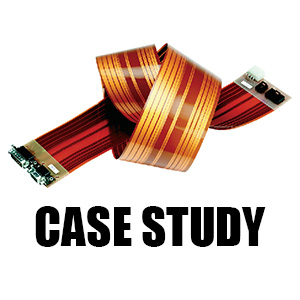
Application: Advantages and Information About ZIF Connectors
There are many types of connectors and termination methods available when designing a flexible circuit. One of the most common is the zero insertion force (ZIF) connector. The reason why the ZIF connector is so popular is that they eliminate the requirement for an added connector. They create a direct connection from the circuit to the mating connector reducing overall weight and cost. Here are a few general facts about ZIF connectors.
1. ZIF Connectors Capabilities and Requirements
- Our equipment allows us to hold ±0.002” tolerance on overall width
- The standard allowable thickness tolerance for 0.012” connectors is ±0.002”
- Specialized material sets have allowed us to hold ±0.001” thickness tolerance on ±0.012” requirement applications verified through multiple capability studies
2. Finishes of ZIF Connectors and Matching With Mating Connector
- Applications that require multiple insertions or greater mechanical force applications (membrane switches) should use hard electrolytic nickel gold (Ni/Au)
- Applications that are static or flex-to-install may only use ENIG/Tin/HASL, depending on the mating connector. It is important to match surface finishes with the contact finishes to inhibit corrosion, especially with tin and gold
- Electroless nickel immersion gold (ENIG) is our most common ZIF plating method and allows for solderability and one surface finish across the entire flex board
3. ZIF Stiffeners
- Polyimide is the most common material added to our standard flex circuit (polyimide) stackup to meet the final ZIF thickness requirement, which is typically 0.012”. Many ZIF connectors have some type of latching mechanism that allows the flex to be inserted and then ultimately clamped down using this latching mechanism
- For ZIF connectors that do not have a latching mechanism, we have utilized an F-R4 (rigid) material as the increased thickness material. The rigid material has the copper etched off which creates a “tooth” for the connector to grab onto versus the polyimide material, which is a smooth material
- ZIF stiffeners are designed to overlap the conductors; 1 mm is the minimum requirement, but 2.5–3 mm is recommended. This provides a “finger hold” for insertion to the connector and prevents mechanical stress and cracking of the conductors. The following images depict the correct design:
Disclaimer
Data presented for informational purposes only. Actual values and/or usage is for reference.
Share on:


Testimonial
"We’re proud to call I-Connect007 a trusted partner. Their innovative approach and industry insight made our podcast collaboration a success by connecting us with the right audience and delivering real results."
Julia McCaffrey - NCAB GroupSuggested Items
WestDev Announces Advanced Thermal Analysis Integration for Pulsonix PCB Design Suite
10/29/2025 | WestDev Ltd.Pulsonix, the industry-leading PCB design software from WestDev Ltd., announced a major enhancement to its design ecosystem: a direct interface between Pulsonix and ADAM Research's TRM (Thermal Risk Management) analysis software.
Designers Notebook: Power and Ground Distribution Basics
10/29/2025 | Vern Solberg -- Column: Designer's NotebookThe principal objectives to be established during the planning stage are to define the interrelationship between all component elements and confirm that there is sufficient surface area for placement, the space needed to ensure efficient circuit interconnect, and to accommodate adequate power and ground distribution.
Episode 6 of Ultra HDI Podcast Series Explores Copper-filled Microvias in Advanced PCB Design and Fabrication
10/15/2025 | I-Connect007I-Connect007 has released Episode 6 of its acclaimed On the Line with... American Standard Circuits: Ultra High Density Interconnect (UHDI) podcast series. In this episode, “Copper Filling of Vias,” host Nolan Johnson once again welcomes John Johnson, Director of Quality and Advanced Technology at American Standard Circuits, for a deep dive into the pros and cons of copper plating microvias—from both the fabricator’s and designer’s perspectives.
Nolan’s Notes: Tariffs, Technologies, and Optimization
10/01/2025 | Nolan Johnson -- Column: Nolan's NotesLast month, SMT007 Magazine spotlighted India, and boy, did we pick a good time to do so. Tariff and trade news involving India was breaking like a storm surge. The U.S. tariffs shifted India from one of the most favorable trade agreements to the least favorable. Electronics continue to be exempt for the time being, but lest you think that we’re free and clear because we manufacture electronics, steel and aluminum are specifically called out at the 50% tariff levels.
MacDermid Alpha & Graphic PLC Lead UK’s First Horizontal Electroless Copper Installation
09/30/2025 | MacDermid Alpha & Graphic PLCMacDermid Alpha Electronics Solutions, a leading supplier of integrated materials and chemistries to the electronics industry, is proud to support Graphic PLC, a Somacis company, with the installation of the first horizontal electroless copper metallization process in the UK.