


 The Right Approach: I Hear the Train A Comin'
 It’s Only Common Sense: OCCAM—the Time Is Now
 Marcy's Musings: The Growing Industry
GaN Systems Releases Best Performance Class-D Amplifier and Companion SMPS Evaluation Kit
May 14, 2020 | GaN SystemsEstimated reading time: 1 minute
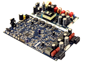
GaN Systems, the global leader in GaN (gallium nitride) power semiconductors, today announced the debut and availability of a new amplifier evaluation kit for high sound quality Class-D audio systems. The evaluation kit includes a 2 channel, 200W per channel (8 ohm) Class-D audio amplifier and companion 400W, continuous power audio-grade SMPS. This solution highlights an easy plug and play design with features such as multi-audio signal inputs, bridge-tied load output, and open-loop/closed-loop toggling. With GaN, the design is very efficient and operates without heatsinks. These features allow audio design engineers to create premium audio products at shorter time to market and at an affordable price.
The convergence of audio trends including demand for more power, size and weight reduction, and growing consumer demand for better audio quality requires innovative approaches to enhance sound quality, increase efficiency, and reduce size which is served by GaN power semiconductors. Applications include smart speakers to automotive and high-end home audio systems.
Evaluation Kit Performance
- 200W/Ch (8?), 300W/Ch (4?) amplifier with 96% efficiency
- 400W continuous, 550W peak companion SMPS
- < 0.01% THD+N (8?, 1W, 20Hz to 20kHz)
- +/?0.5dB frequency response to 50kHz
- High efficiency and no heatsinks, reducing size, weight, and total system cost
- Good EMI/EMC performance due to reduced ringing/noise
“Class-D Audio amplifiers are reaching a new level of performance with GaN. Industry experts and audiophiles alike have tested and listened to the output of our design and are truly impressed,” says Paul Wiener, GaN Systems’ Vice President of Strategic Marketing. “The audio quality combined with the thermal and EMI/EMC performance provide a great solution for our customers.”
Share on:


Suggested Items
iNEMI Packaging Tech Topic Series: Role of EDA in Advanced Semiconductor Packaging
04/26/2024 | iNEMIAdvanced semiconductor packaging with heterogenous integration has made on-package integration of multiple chips a crucial part of finding alternatives to transistor scaling. Historically, EDA tools for front-end and back-end design have evolved separately; however, design complexity and the increased number of die-to-die or die-to-substrate interconnections has led to the need for EDA tools that can support integration of overall design planning, implementation, and system analysis in a single cockpit.
Cadence, TSMC Collaborate on Wide-Ranging Innovations to Transform System and Semiconductor Design
04/25/2024 | Cadence Design SystemsCadence Design Systems, Inc. and TSMC have extended their longstanding collaboration by announcing a broad range of innovative technology advancements to accelerate design, including developments ranging from 3D-IC and advanced process nodes to design IP and photonics.
Ansys, TSMC Enable a Multiphysics Platform for Optics and Photonics, Addressing Needs of AI, HPC Silicon Systems
04/25/2024 | PRNewswireAnsys announced a collaboration with TSMC on multiphysics software for TSMC's Compact Universal Photonic Engines (COUPE). COUPE is a cutting-edge Silicon Photonics (SiPh) integration system and Co-Packaged Optics platform that mitigates coupling loss while significantly accelerating chip-to-chip and machine-to-machine communication.
Siemens’ Breakthrough Veloce CS Transforms Emulation and Prototyping with Three Novel Products
04/24/2024 | Siemens Digital Industries SoftwareSiemens Digital Industries Software launched the Veloce™ CS hardware-assisted verification and validation system. In a first for the EDA (Electronic Design Automation) industry, Veloce CS incorporates hardware emulation, enterprise prototyping and software prototyping and is built on two highly advanced integrated circuits (ICs) – Siemens’ new, purpose-built Crystal accelerator chip for emulation and the AMD Versal™ Premium VP1902 FPGA adaptive SoC (System-on-a-chip) for enterprise and software prototyping.
Listen Up! The Intricacies of PCB Drilling Detailed in New Podcast Episode
04/25/2024 | I-Connect007In episode 5 of the podcast series, On the Line With: Designing for Reality, Nolan Johnson and Matt Stevenson continue down the manufacturing process, this time focusing on the post-lamination drilling process for PCBs. Matt and Nolan delve into the intricacies of the PCB drilling process, highlighting the importance of hole quality, drill parameters, and design optimization to ensure smooth manufacturing. The conversation covers topics such as drill bit sizes, aspect ratios, vias, challenges in drilling, and ways to enhance efficiency in the drilling department.