


 The Chemical Connection: Onshoring PCB Production—Daunting but Certainly Possible
 It’s Only Common Sense: The Phone Is Still Mightier Than the Keyboard


Siemens Acquires Ultrasoc to Drive Design for Silicon Lifecycle Management
June 25, 2020 | PR NewswireEstimated reading time: 2 minutes
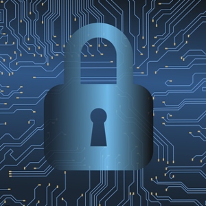
Siemens has signed an agreement to acquire Cambridge, UK-based UltraSoC Technologies Ltd., a provider of instrumentation and analytics solutions that put intelligent monitoring, cybersecurity and functional safety capabilities into the core hardware of system-on-chip (SoC).
Siemens plans to integrate UltraSoC's technology into the Xcelerator portfolio as part of Mentor's Tessent™ software product suite. The addition of UltraSoC to Siemens enables a unified data-driven infrastructure that can enhance product quality, safety and cybersecurity, and the creation of a comprehensive solution to help semiconductor industry customers overcome key pain points including manufacturing defects, software and hardware bugs, device early-failure and wear-out, functional safety, and malicious attacks.
The combination of Siemens and UltraSoC technology can benefit the entire semiconductor product lifecycle, including structural, electrical, and functional capabilities of SoCs.
"Siemens' acquisition of UltraSoC means that for the first time our customers can access not just design-for-test, but a comprehensive 'Design for Lifecycle Management' solution for system-on-chips, including functional safety, security and optimization," says Brady Benware, Tessent Vice President and General Manager, Siemens Digital Industries Software. "By utilizing design augmentation to detect, mitigate and eliminate risks throughout the SoC lifecycle, customers can radically improve time-to-revenue, product quality & safety, and profitability. UltraSoC has a fast-growing business and impressive customer list and, as part of Siemens, can complement Tessent to create a truly unique offering in the market."
UltraSoC is a pioneer of embedding monitoring hardware into complex SoCs to enable "fab-to-field" analytics capabilities designed to accelerate silicon bring-up, optimize product performance, and confirm that devices are operating "as designed" for functional safety and cybersecurity purposes. Tessent is a market leader in SoC design-for-test (DFT) solutions, and has established strengths in the field of automotive functional safety via its Tessent Safety Ecosystem. These two highly complementary offerings are the foundation of a complete package of solutions, encompassing semiconductor design and production, functional safety, cybersecurity, and functional optimization of products in the field.
The combination of Siemens and UltraSoC technology can benefit the entire semiconductor product lifecycle, including structural, electrical, and functional capabilities of SoCs. It also supports Siemens' comprehensive digital twin with UltraSoC providing monitoring of the real device.
"This acquisition accelerates UltraSoC's vision at a much larger scale with the incredible team, assets, industry know-how and footprint of Siemens," said Rupert Baines, CEO, UltraSoC. "Being part of one of the world's foremost technology companies will allow UltraSoC to better serve our customers by accelerating R&D, leveraging a much larger pool of go-to-market resources, and an enormous global infrastructure. It has been clear since our initial meeting that UltraSoC and Siemens share a vision on how technology businesses can transform their operations end-to-end, from design conception to field deployment and we are excited to join the community."
Share on:


Testimonial
"Your magazines are a great platform for people to exchange knowledge. Thank you for the work that you do."
Simon Khesin - Schmoll MaschinenSuggested Items
KYZEN Brings Reliability to Life at productronica 2025 with ANALYST² Process Control Demos
10/22/2025 | KYZEN'KYZEN, the global leader in innovative environmentally responsible cleaning chemistries, will exhibit at productronica 2025, November 18–21 in Munich, Germany, where the company will put a spotlight on its award-winning KYZEN ANALYST² process control system in Hall A4, Stand 450.
SCHMID Group Secures Major Orders for AI Server PCB Production Equipment
10/22/2025 | SCHMID GroupSCHMID Group, a global equipment maker and solution provider for Printed Circuit Boards (PCB) and IC-Substrate manufacturing – announced the successful acquisition of two significant orders in the fast-growing field of PCB for artificial intelligence (AI) server applications. So called AI-Server-Boards.
SEMICON Japan 2025 to Spotlight Sustainability in AI and Semiconductor Innovation
10/22/2025 | SEMISEMICON Japan 2025, the largest gathering of leaders from the microelectronics manufacturing supply chain in Japan, will bring together more than 1,200 exhibitors showcasing semiconductor solutions from December 17-19 at Tokyo Big Sight.
Circus SE Set for High-Volume Market Entry in the Defense Sector
10/17/2025 | BUSINESS WIRECircus SE a global technology leader in AI robotics for autonomous nutrition systems and troop supply, is expanding its global production network as part of its high-volume market entry into the defense sector.
China Expands Rare Earth Export Restrictions, Tightening Grip on Global Supply Chains
10/16/2025 | I-Connect007 Editorial TeamChina sharply expanded its rare earth export restrictions on Oct. 9, adding additional elements and refining technologies to its control list while imposing stricter rules on foreign users in the defense and semiconductor industries.