


 The Chemical Connection: Onshoring PCB Production—Daunting but Certainly Possible
 Marcy’s Musings: The Legislative Outlook—Helping or Hurting?
 It’s Only Common Sense: The Phone Is Still Mightier Than the Keyboard


Plasmatreat Releases Surface Cleaning for a Reliable Wire Bonding Process
October 28, 2020 | PlasmatreatEstimated reading time: 3 minutes
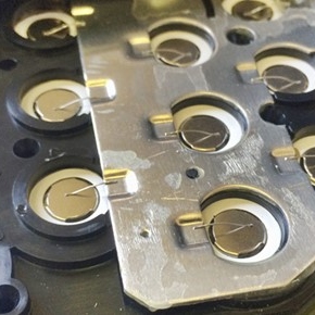
Openair-Plasma from Plasmatreat GmbH is one of the leading technologies worldwide to activate and clean surfaces. It is used in numerous applications to pretreat different substrates. It can also be used to clean metal surfaces for solid wire bonding. The Openair-Plasma technology is a cost-efficient process and can be integrated inline, allowing the bonding process to take place directly after the cleaning is completed.
"Metal can be cleaned using three processes which have different effects and have different treatment goals," says Nico Coenen, Global Business Development Manager Electronics Market of Plasmatreat GmbH, explaining the basic possibilities of plasma treatment. The first process, neutralization, involves the removal of both surface charge and statically bound dirt such as dust particles. This is done by the charge carriers of the Openair-Plasma treatment. In the second process, the volatile components such as moisture and VOCs (volatile organic compounds) are eliminated by evaporation through the thermal effect of the Openair-Plasma treatment. The final cleaning process is removing organic contaminants. The reactive nature of Openair-Plasma causes hydrocarbon chains to be broken down and split into smaller, volatile molecules (up to H2O and CO2).
The successful treatment can be verified, for example, by using an atomic force microscope, which provides visual evidence of the change in the surface. This is a special scanning probe microscope which is used in surface chemistry for mechanical scanning of surfaces and for measuring atomic forces on the nanometer scale. Furthermore, the contact angle method can be used to prove the modified surface tension e.g. by a drop of water. The water drop on the plasma-treated surface changes its wetting properties in such a way that the contact angle and height are reduced and the surface is becoming more hydrophilic.
This is the result of surface cleaning with Openair-Plasma. Especially oxide surfaces, but also contamination caused by bleed out, interfere with the bonding process and prevent reliable connections. Openair-Plasma removes both surface contamination and the oxide layer and the clean surface of the metal alloy is revealed. This is beneficial, in semiconductor applications as particularly clean surfaces are required here in order to reliably bond the ultra-fine wires. The plasma-treated surface allows bonded materials to form a more stable and larger-area connection.
A similar process is used to remove copper oxides, especially in semiconductor and LED applications. By using X-ray photoelectron spectroscopy, the chemical composition of solids and their surface can be determined without causing damage. After treating copper, it can therefore be determined that the surface proportion of copper increases from 3% to 38%, with a concomitant reduction in the carbon content from 43% to 18%. "These changes clearly show that the copper oxide has been reduced and the copper surface area increased," says Coenen. The contact angle analysis also shows a comparable result. Bond wires therefore also form reliable connections here.
In addition to aluminum and copper substrates, nickel surfaces show similarly good properties after being treated with Openair-Plasma. This is particularly important in battery production. Since nickel oxide acts like a barrier layer, which massively complicates the connection with other materials, the cleaning of the nickel surface from oxides is essential. Plasmatreat has therefore developed a special jet for this application that matches the general requirements and at the same time meets the temperature requirements of the process step, for example does not exceed the limit of 50° Celsius.
"The degree to which the individual substrates allow stable wire bonding depends on the material in use. However, the upstream plasma surface treatment improves the application window of the wire bonding process in any case. Both wettability and adhesion are optimized," says Coenen.
Share on:


Testimonial
"Advertising in PCB007 Magazine has been a great way to showcase our bare board testers to the right audience. The I-Connect007 team makes the process smooth and professional. We’re proud to be featured in such a trusted publication."
Klaus Koziol - atgSuggested Items
Episode 6 of Ultra HDI Podcast Series Explores Copper-filled Microvias in Advanced PCB Design and Fabrication
10/15/2025 | I-Connect007I-Connect007 has released Episode 6 of its acclaimed On the Line with... American Standard Circuits: Ultra High Density Interconnect (UHDI) podcast series. In this episode, “Copper Filling of Vias,” host Nolan Johnson once again welcomes John Johnson, Director of Quality and Advanced Technology at American Standard Circuits, for a deep dive into the pros and cons of copper plating microvias—from both the fabricator’s and designer’s perspectives.
Nolan’s Notes: Tariffs, Technologies, and Optimization
10/01/2025 | Nolan Johnson -- Column: Nolan's NotesLast month, SMT007 Magazine spotlighted India, and boy, did we pick a good time to do so. Tariff and trade news involving India was breaking like a storm surge. The U.S. tariffs shifted India from one of the most favorable trade agreements to the least favorable. Electronics continue to be exempt for the time being, but lest you think that we’re free and clear because we manufacture electronics, steel and aluminum are specifically called out at the 50% tariff levels.
MacDermid Alpha & Graphic PLC Lead UK’s First Horizontal Electroless Copper Installation
09/30/2025 | MacDermid Alpha & Graphic PLCMacDermid Alpha Electronics Solutions, a leading supplier of integrated materials and chemistries to the electronics industry, is proud to support Graphic PLC, a Somacis company, with the installation of the first horizontal electroless copper metallization process in the UK.
Electrodeposited Copper Foils Market to Grow by $11.7 Billion Over 2025-2032
09/18/2025 | Globe NewswireThe global electrodeposited copper foils market is poised for dynamic growth, driven by the rising adoption in advanced electronics and renewable energy storage solutions.
MacDermid Alpha Showcases Advanced Interconnect Solutions at PCIM Asia 2025
09/18/2025 | MacDermid Alpha Electronics SolutionsMacDermid Alpha Electronic Solutions, a global leader in materials for power electronics and semiconductor assembly, will showcase its latest interconnect innovations in electronic interconnect materials at PCIM Asia 2025, held from September 24 to 26 at the Shanghai New International Expo Centre, Booth N5-E30