


 Facing the Future: The Role of 5G and Beyond in Shaping PCB Demand
 It’s Only Common Sense: Stop Pitching, Start Listening
 Trouble in Your Tank: Causes of Plating Voids, Pre-electroless Copper


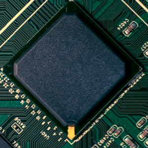
CyberOptics Highlights Best-Practices for Detecting Particles in Semiconductor Environments at SPIE
April 19, 2022 | CyberOptics CorporationEstimated reading time: 1 minute
CyberOptics Corporation, a leading global developer and manufacturer of high-precision 3D sensing technology solutions, will exhibit at SPIE Advanced Lithography and Patterning from April 27-28 at the San Jose Convention Center in California, booth #217. During the show, the company will feature the In-Line Particle Sensor (IPS) and ReticleSense wireless sensors for improved yields and productivity.
An extension of the industry-leading WaferSense and ReticleSense Airborne Particle Sensor (APS) technology that is documented by fabs as the Best Known Method (BKM), the In-Line Particle Sensor (IPS) with CyberSpectrum software detects particles in gas and vacuum lines 24/7. The IPS quickly identifies, monitors and enables troubleshooting of particles down to 0.1µm.
The IPS can be installed in any gas or vacuum system, and it is particularly relevant for EUVL tools where the ability to monitor particles in-line can significantly improve tool yield and productivity. For example, it can be installed at the vacuum line in between the EUV process chamber and the vacuum pump, saving significant time compared to current methods. The IPS is always on and collecting particle data, which is especially critical during chamber purging.
Process and equipment engineers in semiconductor fabs can speed equipment qualification with real-time monitoring, compare past and present data, as well as one tool to another. Contamination sources can be identified quickly and the effects of cleaning, adjustments and repairs can be seen in real-time. Fabs can shorten equipment maintenance cycles, lower equipment expenses and optimize preventative maintenance plans.
CyberOptics will also demonstrate the ReticleSense Airborne Particle Sensor (APSRQ) and the ReticleSense Auto Multi Sensor (AMSR) for wireless leveling, vibration, and relative humidity (RH) measurements.
Share on:


Suggested Items
MKS Breaks Ground on New Chemical Manufacturing and TechCenter Facility in Thailand
05/07/2025 | MKS Instruments, Inc.MKS Instruments. Inc., a global provider of enabling technologies that transform our world, announced today the groundbreaking of its cutting-edge Atotech chemical manufacturing and TechCenter facility at the Asia Industrial Estate Suvarnabhumi, located east of Bangkok, Thailand.
Libra Industries Boosts SMT and Electronics Manufacturing Capabilities in Dallas, Texas
05/06/2025 | Libra IndustriesLibra Industries is excited to announce the latest upgrades to its surface mount technology (SMT) capabilities at its Dallas, Texas facility.
Taiwan's PCB Industry Chain Is Expected to Grow Steadily by 5.8% Annually in 2025
05/05/2025 | TPCAAccording to an analysis report jointly released by the Taiwan Printed Circuit Association (TPCA) and the Industrial Technology Research Institute's International Industrial Science Institute, the total output value of Taiwan's printed circuit (PCB) industry chain will reach NT$1.22 trillion in 2024, with an annual growth rate of 8.1%.
Manncorp Launches Industry-First 'Build Your Own SMT Line' Tool
05/02/2025 | ManncorpManncorp, a leading supplier of SMT (Surface Mount Technology) equipment, proudly announces the official launch of its “Build Your Own SMT Line” tool – a first-of-its-kind resource in the electronics manufacturing industry. Introduced just one month ago, this revolutionary online feature gives manufacturers the unprecedented ability to design a complete SMT production line tailored to their exact needs – all from their desktop.
LG Innotek to Build FC-BGA into 700 Million USD Business with State-of-the-art Dream Factory
05/01/2025 | PR NewswireLG unveiled the Dream Factory, a hub for the production of FC-BGAs (Flip Chip Ball Grid Arrays), the company's next-generation growth engine, to the media for the first time and announced it on the 30th April.