


 Facing the Future: The Role of 5G and Beyond in Shaping PCB Demand
 It’s Only Common Sense: Stop Pitching, Start Listening
 Trouble in Your Tank: Causes of Plating Voids, Pre-electroless Copper


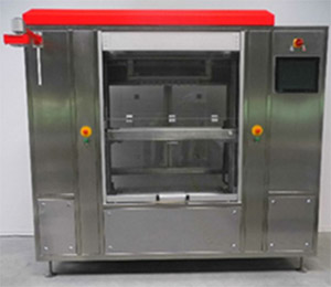
Candor: UHDI Under Development
December 21, 2022 | Nolan Johnson, I-Connect007Estimated reading time: 3 minutes

Candor Industries is a PCB fabricator investing in UHDI fabrication capabilities in Canada. To support advanced packaging, as well as the current pace of IC process shrinks, PCB fabrication capabilities must shrink to keep up. Sunny Patel, Candor’s technical sales manager, brings us up to speed on what Candor has learned in their journey to add UHDI. What we gain from this interview is that, while certainly not insignificant, the stretch to add UHDI may be not as far as one might think.
Nolan Johnson: Sunny, is Candor officially stepping into the realm of UHDI?
Sunny Patel: We’re starting to get there. The first dabbling in UHDI has been these direct on-chip boards that some of our customers are trying to do. Every layer seems sequentially drilled with 2-mil line and space, or 2-mil line with 1.5-mil spacing. We haven’t done a lot of it, but we have seen some demand for it.
Johnson: Where do you draw the line between UHDI and HDI? When does it become UHDI to you?
Patel: For us, UHDI is when it becomes more than sub-drilling and sequential blind vias; it’s a mixture of that, plus sub-3-mil lines/spaces, from my perspective. It becomes case-by-case specific on how to process these boards. I suppose that is the limitation of our equipment, but also our understanding of how things etch differently in that space. The basic tools that you have, the direct imaging, and the really tight registration of your layers are all important. But then you start getting into etch factor adjustments in different areas, like the horns or making sharper square pads, and extreme reduction of copper on the surface becomes very important.
Johnson: Do you need clean room facilities?
Patel: Most board shops use a clean room already or at least the ones I’ve seen; we all have a clean room. On the imaging side, that’s very important, but it’s more than that. It’s a whole new ball game. We’ve done the sequential blind vias, but how do we plate those areas but also limit the copper surface and make sure the etching is still perfect every time for every layer set? The processes are very involved now. You need someone who can look at the data. Based on experience, you know how things are going to etch in that sub-2-mil space and adjust here and there.
Johnson: Is there more custom tuning to get that ready to go?
Patel: Yes, and everyone in that space is experienced with semiconductor-level tolerances. There seems to be a big learning curve for those designers because they’re usually designing with that in mind. There seems to be a bit of a knowledge gap on learning how a circuit board factory works and the limitations of it all.
Johnson: Yes, the dimensions on the silicon 20 years ago weren’t much smaller than the dimensions we’re putting on the boards now. At that point for ICs, we were doing silicon in clean room environments and a great deal of standardization and process work and precision in that which doesn’t seem to have migrated over into the printed circuit board manufacturing industry until now. How close are we to needing to have a clean room environment throughout the facility?
Patel: I’m not entirely sure if we need a clean room for every system. But we need more control. Obviously, the imaging has always been a clean room setup, but the control of the plating and the control of the drilling becomes so much more critical. There doesn’t necessarily need to be a clean room throughout the whole department. For example, with a laser drill you need that vacuum system and the enclosed ventilation system in that kind of equipment whenever you’re doing the actual process.
With plating, it becomes more about chemistry control. The fluid dynamics must be fine-tuned to make sure that you’re even across the panel. That’s what people are transitioning toward, like the knife edge movement vs. the traditional rack movement of plating, enclosed vertical plating lines. So, the systems are becoming more controlled. I don’t know if the whole line must be in a clean room, but it has to be less open to the environment.
To read this entire conversation, which appeared in the November 2022 issue of PCB007 Magazine, click here.
Share on:


Suggested Items
RF PCB Design Tips and Tricks
05/08/2025 | Cherie Litson, EPTAC MIT CID/CID+There are many great books, videos, and information online about designing PCBs for RF circuits. A few of my favorite RF sources are Hans Rosenberg, Stephen Chavez, and Rick Hartley, but there are many more. These PCB design engineers have a very good perspective on what it takes to take an RF design from schematic concept to PCB layout.
Trouble in Your Tank: Causes of Plating Voids, Pre-electroless Copper
05/09/2025 | Michael Carano -- Column: Trouble in Your TankIn the business of printed circuit fabrication, yield-reducing and costly defects can easily catch even the most seasoned engineers and production personnel off guard. In this month’s column, I’ll investigate copper plating voids with their genesis in the pre-plating process steps.
Elephantech: For a Greener Tomorrow
04/16/2025 | Marcy LaRont, PCB007 MagazineNobuhiko Okamoto is the global sales and marketing manager for Elephantech Inc., a Japanese startup with a vision to make electronics more sustainable. The company is developing a metal inkjet technology that can print directly on the substrate and then give it a copper thickness by plating. In this interview, he discusses this novel technology's environmental advantages, as well as its potential benefits for the PCB manufacturing and semiconductor packaging segments.
Trouble in Your Tank: Organic Addition Agents in Electrolytic Copper Plating
04/15/2025 | Michael Carano -- Column: Trouble in Your TankThere are numerous factors at play in the science of electroplating or, as most often called, electrolytic plating. One critical element is the use of organic addition agents and their role in copper plating. The function and use of these chemical compounds will be explored in more detail.
IDTechEx Highlights Recyclable Materials for PCBs
04/10/2025 | IDTechExConventional printed circuit board (PCB) manufacturing is wasteful, harmful to the environment and energy intensive. This can be mitigated by the implementation of new recyclable materials and technologies, which have the potential to revolutionize electronics manufacturing.