


 It’s Only Common Sense: The Phone Is Still Mightier Than the Keyboard
 The Marketing Minute: Marketing With Layers


'No-ink' Color Printing with Nanomaterials
June 8, 2015 | Missouri University of Science and TechnologyEstimated reading time: 3 minutes
Researchers at Missouri University of Science and Technology are giving new meaning to the term “read the fine print” with their demonstration of a color printing process using nanomaterials.
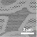
In this case, the print features are very fine – visible only with the aid of a high-powered electron microscope.
The researchers describe their “no-ink” printing method in the latest issue of the Nature Publishing Group journalScientific Reports and illustrate their technique by reproducing the Missouri S&T athletic logo on a nanometer-scale surface. A nanometer is one billionth of a meter, and some nanomaterials are only a few atoms in size.
The method described in the Scientific Reports article “Structural color printing based on plasmonic metasurfaces of perfect light absorption” involves the use of thin sandwiches of nanometer-scale metal-dielectric materials known as metamaterials that interact with light in ways not seen in nature. Experimenting with the interplay of white light on sandwich-like structures, or plasmonic interfaces, the researchers developed what they call “a simple but efficient structural color printing platform” at the nanometer-scale level. They believe the process holds promise for future applications, including nanoscale visual arts, security marking and information storage.
The researchers’ printing surface consists of a sandwich-like structure made up of two thin films of silver separated by a “spacer” film of silica. The top layer of silver film is 25 nanometers thick and is punctured with tiny holes created by a microfabrication process known as focused ion beam milling. The bottom layer of silver is four times thicker than the top layer but still minuscule at 100 nanometers. Between the top and bottom films lies a 45-nanometer silica dielectric spacer.
The researchers created a scaled-down template of the athletic logo and drilled out tiny perforations on the top layer of the metamaterial structure. Under a scanning electron microscope, the template looks like a needlepoint pattern of the logo. The researchers then beamed light through the holes to create the logo using no ink – only the interaction of the materials and light.
By adjusting the hole size of the top layer, light at the desired frequency was beamed into the material with a perfect absorption. This allowed researchers to create different colors in the reflected light and thereby accurately reproduce the S&T athletic logo with nanoscale color palettes. The researchers further adjusted the holes to alter the logo’s official green and gold color scheme to introduce four new colors (an orange ampersand, magenta “S” and “T,” cyan pickaxe symbol and navy blue “Missouri”).
“To reproduce a colorful artwork with our nanoscale color palettes, we replaced different areas in the original image with different nanostructures with specified hole sizes to represent various visible colors,” says Dr. Xiaodong Yang, an assistant professor at Missouri S&T, who leads the Nanoscale Optics Laboratory in the university’s mechanical and aerospace engineeringdepartment. “We chose the athletic logo to fill that need.”
“Unlike the printing process of an inkjet or laserjet printer, where mixed color pigments are used, there is no color ink used in our structural printing process – only different hole sizes on a thin metallic layer,” says Dr. Jie Gao, an assistant professor of mechanical and aerospace engineering at Missouri S&T and a co-author of the paper.
In their paper, the authors note that the process resulted in “pure colors with high brightness” with little need for protective coatings. The researchers believe the process could lead to “high-performance, pigment-free color printing and relevant applications such as security marking and information storage.”
Other co-authors of the Scientific Reports paper are Dr. Fei Cheng, a researcher at Missouri S&T’s Nanoscale Optics Laboratory, and Dr. Ting S. Luk of the Center for Integrated Nanotechnologies at Sandia National Laboratories in Albuquerque, New Mexico.
Share on:


Testimonial
"We’re proud to call I-Connect007 a trusted partner. Their innovative approach and industry insight made our podcast collaboration a success by connecting us with the right audience and delivering real results."
Julia McCaffrey - NCAB GroupSuggested Items
The Republic of Korea Selects L3Harris for Airborne Early Warning and Control Aircraft Program
10/20/2025 | BUSINESS WIREL3Harris Technologies has received a contract to deliver modified Bombardier Global 6500 airborne early warning and control (AEW&C) aircraft to the Republic of Korea Air Force.
Molex Announces Agreement to Acquire Smiths Interconnect
10/17/2025 | MolexMolex, a leading global electronics connectivity innovator, announced that it has signed an agreement to acquire Smiths Interconnect.
American Standard Circuits Achieves Successful AS9100 Recertification
10/14/2025 | American Standard CircuitsAmerican Standard Circuits (ASC), a leading manufacturer of advanced printed circuit boards, proudly announces the successful completion of its AS9100 recertification audit. This milestone reaffirms ASC’s ongoing commitment to the highest levels of quality, reliability, and process control required to serve aerospace, defense, space, and other mission-critical industries.
Kodiak Assembly Solutions Renews ITAR Registration, Providing Secure and Compliant Manufacturing for Defense & Aerospace
09/25/2025 | Kodiak Assembly SolutionsKodiak Assembly Solutions LLLP, a leading electronics contract manufacturer, has successfully renewed its ITAR (International Traffic in Arms Regulations) registration.
Cyient DLM, A Voice from the Frontlines
09/24/2025 | Arpita Das, Global Electronics AssociationOnce seen as a low-cost, build-to-print destination, India’s EMS sector is rapidly emerging as a global hub for high-reliability electronics, particularly in strategic sectors like aerospace, defense, and medical. As such, we highlight some companies that exemplify the strength and potential of Indian manufacturing.