Punching Out: M&A Deals in North American PCB and EMS Sectors for the First Half of 2026
 Trouble in Your Tank: At 40 GHz, Everything Matters, Part 2
 It’s Only Common Sense: Stop Watching the Headlines and Start Watching the Opportunity


Major advances in the field of organic electronics are currently revolutionising previously silicon-dominated semiconductor technology. Customised organic molecules enable the production of lightweight, mechanically flexible electronic components that are perfectly adapted to individual applications. Chemists at the Goethe University have now developed a new class of organic luminescent materials through the targeted introduction of boron atoms into the molecular structures. The compounds described in the professional journal "Angewandte Chemie" (Applied Chemistry) feature an intensive blue fluorescence and are therefore of interest for use in organic light-emitting diodes (LED's).
Carbon in the form of graphite conducts the electrical current in a similar way to a metal. In addition, its two-dimensional shape, the graphene layer, has extremely attractive optical and electronic properties. In graphene, the discoverers of which were awarded the Nobel Prize for Physics in 2010, countless benzene rings are fused to form a honeycomb structure. Sections of this structure, so-called nanographenes or Polycyclic Aromatic Hydrocarbons (PAHs), constitute an important basis of organic electronics.
"For a long time, efforts were largely focused on affecting the properties of nanographenes by chemically manipulating their edges", according to Prof. Matthias Wagner of the Institute for Inorganic and Analytical Chemistry at the Goethe University. "However, in recent years, researchers have been increasingly capable of also modifying the inner structure by embedding foreign atoms in the carbon network. This is where boron assumes crucial significance."
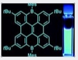
A comparison of the new boron-containing nanographenes with the analogous boron-free hydrocarbons verifies the fact that the boron atoms have a decisive impact on two key properties of an OLED luminophore: the fluorescence colour shifts into the highly desirable blue spectral range and the capacity to transport electrons is substantially improved. To date, only limited use could be made of the full potential of boron-containing PAHs, since most of the exponents are sensitive to air and moisture. "This problem does not occur with our materials, which is important with regard to practical applications" explains Valentin Hertz, who synthesised the compounds within the scope of his doctoral dissertation.
Hertz and Wagner anticipate that materials such as the graphene flakes they have developed will be particularly suitable for use in portable electronic devices. As film displays for future generations of smartphones and tablets, even large-scale screens could be rolled up or folded to save space when the devices are not in use.
New Boron Compounds for OLEDs
| Goethe-UniversityEstimated reading time: 2 minutes