


 The Right Approach: I Hear the Train A Comin'
 It’s Only Common Sense: OCCAM—the Time Is Now
 Marcy's Musings: The Growing Industry
UCSB Becomes West Coast Hub for National Photonics Manufacturing Institute
July 30, 2015 | UCSBEstimated reading time: 4 minutes
In a bid to boost photonics manufacturing and bring more skilled, high-tech jobs to the country, as well as push the boundaries of energy efficiency and performance in computing and telecommunications, the Obama administration announced today that it has selected the American Institute for Manufacturing of Photonics (AIM Photonics) to lead research and manufacturing of integrated photonic technology and create jobs in this important area. UC Santa Barbara is leading the West Coast division of this public-private partnership, in collaboration with the State University of New York — the lead university in this institute.
In the age of the Internet and Big Data, conventional electronic technology — even with the advent of Moore’s Law, which predicts the doubling of transistors and processing power approximately every two years — will become overwhelmed by the demand for speed, performance and data capacity.
The solution to that impending demand lies in photonics, the use of light to transmit massive amounts of data at extremely high speeds. But to make the shift between electronic wires and photonic waveguides, the two technologies must be brought together.
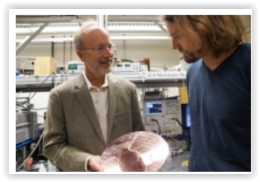
“AIM and UC Santa Barbara are leading a revolution that is integrating photonics and electronics for the benefits of both,” said John Bowers, professor of electrical and computer engineering and of materials at UCSB, director of the campus’s Institute for Energy Efficiency (IEE) and lead of the West Coast hub of AIM. Just as photonics has enabled the fiber optic communications which led to the Internet revolution, he said, the increased data capacity, speed and energy efficiency promised by photonics integrated circuits will result in enormous gains for everything from handheld devices to personal computing to data centers. “Our goal is to use complementary metal-oxide semiconductor processing to move photonics onto silicon and accelerate the integration of photonics and eliminate the data bottleneck that advanced silicon chips are facing during the next decade,” said Bowers.
“UC Santa Barbara has been a leader in integrated photonics for the past 30 years,” said UCSB Chancellor Henry T. Yang, “and this has been recognized in numerous ways, especially by three Nobel prizes: one in physics to Herb Kroemer, inventor of the double heterostructure laser, which is used in all data communications and telecom systems worldwide; one in chemistry to Alan Heeger, inventor of conductive polymers, which are widely used for displays and photovoltaic devices; and another one in physics to Shuji Nakamura, inventor of the blue LED, which is widely used for lighting.” Add to this roster of groundbreaking UCSB researchers John Bowers — considered to be one of the world’s foremost authorities in optoelectronics — whose work in the IEE seeks to provide energy efficient solutions for computing while also improving performance.
UC President Janet Napolitano said the announcement reflects how UC research advances the economic strength of both California and the nation.
“The exciting news about UC Santa Barbara serving as the West Coast hub for AIM Photonics, an Obama Administration initiative, is another testament to the value of the University of California’s research enterprise,” Napolitano said. “In this case, research by a consortium that includes our Santa Barbara, Davis, Berkeley and San Diego campuses is pushing the boundaries of energy efficiency and performance in computing and telecommunications. The research is attracting significant federal funding, as well as state and private funds, that will help create significant economic impact.”
To create a successful end-to-end integrated photonics manufacturing ecosystem in the U.S., research must be amplified, the technology supplied and a workforce trained. AIM will leverage its federal, state and private funding to expand upon already existing partnerships between research and industry to align efforts and share resources to meet the needs of this emerging industry.
With the $110 million in funding from the government, the new consortium aims to align research strength with development prowess to revitalize critical sectors of the country’s manufacturing economy. Universities, including the Massachusetts Institute of Technology, University of Arizona, Stanford University, California Institute of Technology, UC Davis, UC Berkeley, UC San Diego, Columbia University and the University of Virginia will contribute their considerable research to the consortium. Meanwhile, major integrated photonics companies such as Intel, Hewlett Packard, Infinera, Agilent, Lockheed and Raytheon as well as design software companies Synopsys, Mentor and Cadence will lead the manufacturing charge.
According to Rod Alferness, dean of the College of Engineering, UCSB already has the momentum to bring cutting-edge research and software tools for design into the manufacturing and commercial sphere. “UCSB is a worldwide leader in integrating lasers onto silicon,” he said. “Many new companies have spun out of our photonics research, including Aurrion, Agility, Calient Networks, Soraa, Aerius Photonics and Freedom Photonics.”
“Today’s announcement is a testament to the outstanding team of industrial and academic leaders assembled by AIM Photonics and its plan to establish the U.S. as a global leader in this emerging technology. Being awarded the Integrated Photonics Institute for Manufacturing Innovation (IP-IMI) would not have been possible without the critical support of Governor Andrew Cuomo, whose pioneering leadership in establishing New York State’s globally recognized, high-tech R&D ecosystem has enabled historic economic growth and innovation and secured our partnership with the state of California,” said Dr. Michael Liehr, AIM CEO and SUNY Poly Executive Vice President of Innovation and Technology and Vice President of Research. “SUNY Poly is excited to be working with partners such as UC Santa Barbara on this initiative which will be truly transformational for both the industry and the nation.”
Share on:


Suggested Items
Real Time with… IPC APEX EXPO 2024: Tools, Training, and Trends in Manufacturing Engineering
04/25/2024 | Real Time with...IPC APEX EXPOGuest Editor Kelly Dack and Product Specialist Erik Bateham of Polar Instruments discuss Polar's latest technology, including their role in aiding manufacturing engineers. They highlight the advanced capabilities of Polar's tools and the critical role of signal integrity analysis, as well as the importance of accurate modeling in board manufacturing. Polar's unique training approach and demonstration contact details are also explored.
TTM Celebrates the Grand Opening of Its First Manufacturing Facility in Penang
04/25/2024 | TTM Technologies, Inc.TTM Technologies, Inc., a leading global manufacturer of technology solutions including mission systems, radio frequency (RF) components and RF microwave/microelectronic assemblies, and quick-turn and technologically advanced printed circuit boards (PCBs), officially opened its first manufacturing plant in Penang, Malaysia with an investment of USD200 million (approximately RM958 million).
Listen Up! The Intricacies of PCB Drilling Detailed in New Podcast Episode
04/25/2024 | I-Connect007In episode 5 of the podcast series, On the Line With: Designing for Reality, Nolan Johnson and Matt Stevenson continue down the manufacturing process, this time focusing on the post-lamination drilling process for PCBs. Matt and Nolan delve into the intricacies of the PCB drilling process, highlighting the importance of hole quality, drill parameters, and design optimization to ensure smooth manufacturing. The conversation covers topics such as drill bit sizes, aspect ratios, vias, challenges in drilling, and ways to enhance efficiency in the drilling department.
Elevating PCB Design Engineering With IPC Programs
04/24/2024 | Cory Blaylock, IPCIn a monumental stride for the electronics manufacturing industry, IPC has successfully championed the recognition of the PCB Design Engineer as an official occupation by the U.S. Department of Labor (DOL). This pivotal achievement not only underscores the critical role of PCB design engineers within the technology landscape, but also marks the beginning of a transformative journey toward nurturing a robust, skilled workforce ready to propel our industry into the future.
Fujitsu, METRON Collaborate to Drive ESG Success
04/24/2024 | JCN NewswireFujitsu Limited and METRON SAS, a French cleantech company specializing in energy management solutions for industrial decarbonization, today announced a strategic initiative to contribute to the realization of carbon neutrality in the manufacturing industry.