


 The Right Approach: I Hear the Train A Comin'
 It’s Only Common Sense: OCCAM—the Time Is Now
 Marcy's Musings: The Growing Industry
Nano Dimension Launches 3D Printer Dedicated to Ultra-Rapid Prototyping of PCBs
November 18, 2015 | Business WireEstimated reading time: 2 minutes
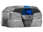
Nano Dimension Ltd. today revealed the world’s first desktop-sized 3D printer designed specifically for the production of professional multilayer printed circuit boards (PCBs). The DragonFly 2020 3D Printer, being demonstrated in the US for the first time at the Printed Electronics USA 2015 conference (Booth F09), will allow users to build functional, multilayer circuit board prototypes in-house –in a matter of hours.
The capability of rapidly producing functional multilayer PCB prototypes using 3D printing is new to the printed electronics design and manufacturing industry. The current standard subtractive manufacturing of PCBs is a multi-stage, labor- and material-intensive process, and is so costly and time consuming that electronics designers requiring prototypes resort to outsourcing. Nano Dimension’s 3D printer can print a complete multilayer PCB, including all interconnections between layers, using its revolutionary inkjet printer and highly conductive nano-inks. Sophisticated proprietary software accepts industry standard Gerber design files and manages the precise print process. In addition, the DragonFly 2020 3D Printer gives users the option of testing on-the-fly, testing a range of designs and exploring new circuit geometries.
The DragonFly 2020 3D Printer is a three-axis inkjet printer; its benefits and attributes include:
- On-site ultra-rapid prototyping of professional multilayer prototype PCBs including interconnections and through-holes.
- Reduced PCB design and test cycles, from months or weeks to days.
- Minimize costs and inexpensively evaluate design alternatives and creative ideas.
- Security of IP, sensitive design information stays in-house.
- A greener alternative to standard PCB production since it is a cleaner process with no waste.
- Compact, office-friendly 3D printer.
“For designers and engineers looking for ultra-rapid prototyping of PCBs, our 3D printer is a significant leap forward. The DragonFly 3D Printer eliminates the frustration they face when they reach the prototyping and testing stage,” said Simon Fried, Chief Marketing Officer at Nano Dimension. “Moving their work from design to a prototype at an off-site printing facility might take weeks for the PCB to be ordered, produced and shipped. If further iterations are needed, it’s back to the prototyping house for another cycle. In today’s competitive electronics markets, unforeseeable and costly delays during PCB development can significantly slow time-to-market. That’s the development risk and bottleneck that we’re eliminating with the DragonFly 2020.”
At Printed Electronics USA, Nano Dimension is also exhibiting its AgCite line of conductive silver nanoparticle inks for inkjet deposition and 3D printed PCB prototype samples. In addition, Nano Dimension’s CMO Simon Fried will give a presentation on “What happens when 3D printing and conductive inks converge?”
The DragonFly 2020 3D Printer is targeted for commercial availability during the second half of 2016. The AgCite conductive inks are available today.
About Nano Dimension
Nano Dimension, founded in 2012, focuses on the development of advanced 3D printed electronics systems. Nano Dimension's unique products combine three advanced technologies: 3D inkjet, 3D software and nanomaterials. The company's primary products include the first 3D printer dedicated to printing multilayer PCBs (printed circuit boards) and advanced nanotechnology-based conductive and dielectric inks.
Share on:


Suggested Items
Warm Windows and Streamlined Skin Patches – IDTechEx Explores Flexible and Printed Electronics
04/26/2024 | IDTechExFlexible and printed electronics can be integrated into cars and homes to create modern aesthetics that are beneficial and easy to use. From luminous car controls to food labels that communicate the quality of food, the uses of this technology are endless and can upgrade many areas of everyday life.
Book Excerpt: The Printed Circuit Assembler’s Guide to... Factory Analytics
04/24/2024 | I-Connect007 Editorial TeamIn our fast-changing, deeply competitive, and margin-tight industry, factory analytics can be the key to unlocking untapped improvements to guarantee a thriving business. On top of that, electronics manufacturers are facing a tremendous burden to do more with less. If you don't already have a copy of this book, what follows is an excerpt from the introduction chapter of 'The Printed Circuit Assembler’s Guide to... Factory Analytics: Unlocking Efficiency Through Data Insights' to whet your appetite.
Listen Up! The Intricacies of PCB Drilling Detailed in New Podcast Episode
04/25/2024 | I-Connect007In episode 5 of the podcast series, On the Line With: Designing for Reality, Nolan Johnson and Matt Stevenson continue down the manufacturing process, this time focusing on the post-lamination drilling process for PCBs. Matt and Nolan delve into the intricacies of the PCB drilling process, highlighting the importance of hole quality, drill parameters, and design optimization to ensure smooth manufacturing. The conversation covers topics such as drill bit sizes, aspect ratios, vias, challenges in drilling, and ways to enhance efficiency in the drilling department.
Elevating PCB Design Engineering With IPC Programs
04/24/2024 | Cory Blaylock, IPCIn a monumental stride for the electronics manufacturing industry, IPC has successfully championed the recognition of the PCB Design Engineer as an official occupation by the U.S. Department of Labor (DOL). This pivotal achievement not only underscores the critical role of PCB design engineers within the technology landscape, but also marks the beginning of a transformative journey toward nurturing a robust, skilled workforce ready to propel our industry into the future.
Winner of The Science Show Rakett 69 Receives Incap Scholarship
04/24/2024 | IncapThe winner of the Rakett 69 science show, Andri Türkson, who stood out as an electronics enthusiast, received a scholarship from Incap Estonia, along with an internship opportunity in Saaremaa.