


 Driving Innovation: Mechanical and Optical Processes During Rigid-flex Production
 It’s Only Common Sense: Your Biggest Competitor Is Complacency
 The Chemical Connection: Onshoring PCB Production—Daunting but Certainly Possible


World's Largest Flexible X-Ray Detector
December 31, 2015 | Arizona State UniversityEstimated reading time: 1 minute
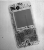
The Flexible Electronics and Display Center (FEDC) at Arizona State University and PARC, a Xerox company, announced that they have successfully manufactured the world's largest flexible X-ray detector prototypes using advanced thin film transistors.
Measuring 10 diagonal inches, the device has been jointly developed at the ASU center and PARC in conjunction with the Army Research Lab and the Defense Threat Reduction Agency. The device will be used to advance the development of flexible X-ray detectors for use in thin, lightweight, conformable and highly rugged devices.
"This achievement is a fantastic example of how academia, industry and government can collaborate to advance key technologies and national priorities," said Sethuraman "Panch" Panchanathan, senior vice president for Knowledge Enterprise Development at ASU.
"Flexible electronics hold tremendous potential to accelerate our global competitiveness in the area of advanced manufacturing by partnering with federal agencies and industry leaders."
The thin film transistor and PIN diode processing was done on the 470- by 370-mm Gen II line at the Flexible Electronics and Display Center. This device showcases the center's successful scale up to GEN II, and the ability to produce sensors and displays using thin film transistors in standard process flows with the center's proprietary bond/de-bond technology. These detectors are unique in that they showcase both of the flexible substrates the center uses to make devices. Some of the new detectors are on polyethylene naphthalate and some are on polyimide. Printed and Flexible Sensors 2015-2025 "This success came from a rewarding collaboration that combines FEDC's flexible array fabrication technology and PARC's experience with digital X-ray systems," said Bob Street, PARC Senior Research Fellow.
The system design and integration was done at PARC. The flexible X-ray sensor was coupled to a tablet device for control and image viewing. This system shows PARC's capability to build user-defined prototype systems incorporating novel device physics, materials and technology. PARC has extensive experience in building large-area electronic systems, display and backplane prototypes, and organic and printed electronics.
Share on:


Testimonial
"We’re proud to call I-Connect007 a trusted partner. Their innovative approach and industry insight made our podcast collaboration a success by connecting us with the right audience and delivering real results."
Julia McCaffrey - NCAB GroupSuggested Items
Henger Microelectronics Expands Global Footprint with Major Equipment Shipment to Southeast Asia
10/31/2025 |Henger Microelectronics has reached a major milestone in its global expansion strategy with the successful shipment of advanced plasma etching and cleaning systems, along with automation equipment, to multiple countries and regions across Southeast Asia. This achievement marks a significant step forward in the company’s international growth and reinforces its position as a leading force in the global plasma equipment industry.
TTCI Brings Hands-On Test Engineering and IPC Training Expertise to PCB Carolina 2025
10/31/2025 | The Test Connection Inc.The Test Connection Inc. (TTCI), a trusted provider of electronic test and manufacturing solutions, and The Training Connection LLC (TTC-LLC) will exhibit at PCB Carolina on Wednesday, November 12, 2025, at the McKimmon Center at NC State University in Raleigh, North Carolina. Attendees can visit Table 4 to say hello to Bert Horner and Bill Graver, and learn more about their test engineering services and technical training programs.
Cephia Secures $4M Seed Funding to Revolutionize Multimodal Sensing with Metasurface Technology
10/31/2025 | PRNewswireCephia, a startup building products using advanced AI computational imaging technologies and silicon sensors made from advanced metamaterials, formally launched with several pilot customers and $4 million in seed venture capital funding.
I-Connect007 Editor’s Choice: Five Must-Reads for the Week
10/31/2025 | Nolan Johnson, I-Connect007Last week, the IMPACT conference took place in Taipei, bringing together advanced packaging experts from around the globe to share their knowledge. We’ll be bringing you post-conference coverage over the next few weeks, so look for that in our newsletters, and in the Advanced Electronic Packaging Digest. Other news seemed to have the U.S. at the center of the global discussions. My picks start in Phoenix, where TSMC, NVIDIA, and Amkor are all scrambling to establish new capabilities. There’s nothing like a strong demand signal to cause build-out, and AI chips are doing exactly that.
NEDME 2025 Draws Strong Northwest Crowd, Builds on Tradition of Regional Collaboration
10/31/2025 | NEDMEThe NW Electronics Design & Manufacturing Expo (NEDME) 2025 once again brought together the Pacific Northwest community for a full day of learning, networking, and industry connections.