


 Driving Innovation: Mechanical and Optical Processes During Rigid-flex Production
 It’s Only Common Sense: Your Biggest Competitor Is Complacency
 The Chemical Connection: Onshoring PCB Production—Daunting but Certainly Possible


Researchers Engineer an Electronics First, Opening Door to Flexible Electronics
February 10, 2016 | University of AlbertaEstimated reading time: 3 minutes
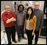
An engineering research team at the University of Alberta has invented a new transistor that could revolutionize thin-film electronic devices.
Their findings, published in the prestigious science journal Nature Communications, could open the door to the development of flexible electronic devices with applications as wide-ranging as display technology to medical imaging and renewable energy production.
The team was exploring new uses for thin film transistors (TFT), which are most commonly found in low-power, low-frequency devices like the display screen you’re reading from now. Efforts by researchers and the consumer electronics industry to improve the performance of the transistors have been slowed by the challenges of developing new materials or slowly improving existing ones for use in traditional thin film transistor architecture, known technically as the metal oxide semiconductor field effect transistor (MOSFET).
But the U of A electrical engineering team did a run-around on the problem. Instead of developing new materials, the researchers improved performance by designing a new transistor architecture that takes advantage of a bipolar action. In other words, instead of using one type of charge carrier, as most thin film transistors do, it uses electrons and the absence of electrons (referred to as “holes”) to contribute to electrical output. Their first breakthrough was forming an ‘inversion’ hole layer in a ‘wide-bandgap’ semiconductor, which has been a great challenge in the solid-state electronics field.
Once this was achieved, “we were able to construct a unique combination of semiconductor and insulating layers that allowed us to inject “holes” at the MOS interface,” said Gem Shoute, a PhD student in the Department of Electrical and Computer Engineering who is lead author on the article. Adding holes at the interface increased the chances of an electron “tunneling” across a dielectric barrier. Through this phenomenon, a type of quantum tunnelling, “we were finally able to achieve a transistor that behaves like a bipolar transistor.”
“It’s actually the best performing [TFT] device of its kind—ever,” said materials engineering professor Ken Cadien, a co-author on the paper. “This kind of device is normally limited by the non-crystalline nature of the material that they are made of”
The dimension of the device itself can be scaled with ease in order to improve performance and keep up with the need of miniaturization. An advantage that modern TFTs lack. The transistor has power-handling capabilities at least 10 times greater than commercially produced thin film transistors.
Electrical engineering professor Doug Barlage, who is Shoute’s PhD supervisor and one of the paper’s lead authors, says his group was determined to try new approaches and break new ground. He says the team knew it could produce a high-power thin film transistor—it was just a matter of finding out how.
“Our goal was to make a thin film transistor with the highest power handling and switching speed possible. Not many people want to look into that, but the raw properties of the film indicated dramatic performance increase was within reach,” he said. “The high quality sub 30 nanometre (a human hair is 50 nanometres wide) layers of materials produced by Professor Cadien’s group enabled us to successfully try these difficult concepts”
In the end, the team took advantage of the very phenomena other researchers considered roadblocks.
“Usually tunnelling current is considered a bad thing in MOSFETs and it contributes to unnecessary loss of power, which manifests as heat,” explained Shoute. “What we’ve done is build a transistor that considers tunnelling current a benefit.”
The team has filed a provisional patent on the transistor. Shoute says the next step is to put the transistor to work “in a fully flexible medium and apply these devices to areas like biomedical imaging, or renewable energy.”
Share on:


Testimonial
"In a year when every marketing dollar mattered, I chose to keep I-Connect007 in our 2025 plan. Their commitment to high-quality, insightful content aligns with Koh Young’s values and helps readers navigate a changing industry. "
Brent Fischthal - Koh YoungSuggested Items
Sealed for Survival: Potting Electronics for the Toughest Environments
10/29/2025 | Beth Massey, MacDermid Alpha Electronics SolutionsElectronics deployed in harsh conditions face relentless threats from vibration, impact, chemical contaminants, airborne pollutants, and moisture, conditions that can quickly lead to failure without robust protection. Potting, the process of encapsulating electronics in a protective polymer, is a widely used strategy to safeguard devices from both environmental and mechanical hazards.
Driving Innovation: Mechanical and Optical Processes During Rigid-flex Production
10/28/2025 | Kurt Palmer -- Column: Driving InnovationRigid-flex printed circuit boards are a highly effective solution for placing complex circuitry in tight, three-dimensional spaces. They are now indispensable across a range of industries, from medical devices and aerospace to advanced consumer electronics, helping designers make the most efficient use of available space. However, their unique construction—combining rigid and flexible materials—presents a fundamental challenge for PCB manufacturers.
SMTAI 2025 Review: Reflecting on a Pragmatic and Forward-looking Industry
10/27/2025 | Marcy LaRont, I-Connect007Leaving the show floor on the final afternoon of SMTA International last week in Rosemont, Illinois, it was clear that the show remains a grounded, technically driven event that delivers a solid program, good networking, and an easy space to commune with industry colleagues and meet with customers.
ITW EAE Despatch Ovens Now Support ASTM 5423 Testing
10/15/2025 | ITW EAEAs the demand for high-performance electrical insulation materials continues to grow—driven by the rapid expansion of electric vehicles (EVs) and energy storage systems—thermal processing has become a critical step in material development.
Beyond Thermal Conductivity: Exploring Polymer-based TIM Strategies for High-power-density Electronics
10/13/2025 | Padmanabha Shakthivelu and Nico Bruijnis, MacDermid Alpha Electronics SolutionsAs power density and thermal loads continue to increase, effective thermal management becomes increasingly important. Rapid and efficient heat transfer from power semiconductor chip packages is essential for achieving optimal performance and ensuring long-term reliability of temperature-sensitive components. This is particularly crucial in power systems that support advanced applications such as green energy generation, electric vehicles, aerospace, and defense, along with high-speed computing for data centers and artificial intelligence (AI).