


 It’s Only Common Sense: Stop Pitching, Start Listening
 Trouble in Your Tank: Causes of Plating Voids, Pre-electroless Copper
 Dan’s Biz Bookshelf: ‘Growth Hacker Marketing’


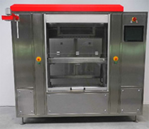
Orbotech’s New Products and Equipment Offerings Highlighted at HKPCA
February 12, 2016 | OrbotechEstimated reading time: 11 minutes

At the recent HKPCA show, members of the media and some of the leading figures at Orbotech joined together for a Q&A session to learn more about some of the company’s new product rollouts, how their vast equipment offering has set them up to take on Industry 4.0, and their best estimate on when we’ll see 3D printed circuit boards reach mass production levels.
Q: What equipment is Orbotech highlighting here at the HKPCA show this year?
Meny Gantz: One highlight of the show is our Diamond 8 direct imaging system for mass production. It is based on our solder mask technology for high throughput, high depth-of-focus and a high capacity for the solder mask makers, reducing their total cost of the ownership and making their product have higher yields. The second product is the Sprint 200, which is entering in a new domain of mass production legend printing. With this system we are achieving very fast throughputs almost comparable to silkscreen, making this a very good alternative for producers of PCBs.
Q: In the China market, the cost of production is a very sensitive topic. How will Orbotech take care of this cost-sensitive industry and can your equipment answer this trend? The second question is about PCB manufacturing in the China market. Do you expect there will still be growth in China or do you see production moving to Southeast Asia?
Gaby Waisman: That's a very good question. I want to start with the second question and then relate back to the first one. First of all, China is obviously the biggest production hub for PCBs in the world. There is a very established ecosystem around the production of PCBs here. In the foreseeable future, I don't see the production base that the PCB industry has in China being jeopardized. Obviously there are PCB manufacturers that have established their production bases in countries such as Vietnam, Thailand and Malaysia. We are definitely supporting the customers in those countries and, as always, there’s an industry dynamic of exploring places in which PCBs could be produced more cost efficiently. With that said, even with the establishment of the bases in the countries I mentioned, I see most of the forecast and growth and investment being in Mainland China, both in terms of ecosystem as well as the capital equipment, at least for the foreseeable future.
Coming back to your first question, this year Orbotech will invest close to $100,000,000 in R&D. R&D is at our core. This is part of the Orbotech DNA and we excel by differentiating ourselves in two main areas, technology and innovation. However, technology and innovation have a purpose. The purpose is essentially to improve the three main factors in PCB production: yield, efficiency and eventually cost of production. So the focus of Orbotech is how to leverage this R&D money into bringing both cost of production down, as well as offering digital production capabilities to areas that are currently not using such advanced digital tools in order to have better efficiencies. This is in line with the trend of automation and with other trends associated with higher labor costs in China and the needs of the PCB industry in general.
Last but not least, and close to all of our hearts, are areas that relate to the environment. Moving to digital has other advantages, and some of those advantages have to do with the environment. For example, lower consumption of electricity, less floor space, etc. In the inkjet environment, having higher utilization of the ink rather than utilizing a lot of ink in the current silkscreen solution has the ability to save on ink, not only in terms of cost but also in terms of the environment. Much of the investment that we have in our products has to do with the cost of production obviously, but also with other very relevant factors to each and everyone's lives today.
Q: How long will it be before Orbotech is just printing circuit boards out of a single machine?
Waisman: I'll start by saying that the key thing we need to consider here is the designers. What are the designers’ ambitions? What are their dreams? How does the PCB industry, and how do we, as part of the suppliers in the PCB industry, help them realize their dreams? They wake up in the morning and think about the next big consumer electronic gadget. They wake up and ask themselves how they can make it smaller, faster, better, or friendlier. Whether that relates to the Internet of Things, the smartphone industry, or automotive and so on, the reason we wake up each morning and think about how to improve and provide better tools is to fulfill for our customers their designers’ dreams. That is one axis. The other axis is obviously the cost of doing that and the trends in general. It has to do with automation, becoming greener and other environmental considerations, and it has to do with basic capabilities that we need to address soon.
We are basically queued to serve this ecosystem and to fulfill those dreams for our customers. Concerning the other question related to 3D inkjet printing, I would say that we realize that there is a dream of perhaps making PCBs differently. We are part of that dream, but we don't necessarily see that happening in the short term, for mass production, due to the cost structure of our customers' specs. The dreaming is definitely something we share in, and the 3D industry is evolving very fast, but I believe that we are still quite far from realizing this dream in mass production.
Q: How many years away do you think it is?
Waisman: Very good question. I don’t think it’s in the very near future, but I can definitely see something in the mid- to long-term timeframe happening. It is very difficult to foresee.
Gantz: I agree with what Gaby just mentioned. For 3D, there is still a lot of work to be done, mainly on cost structure and the ability to do it in mass production. For your first question about automation, yes we see it happening and we are part of it. All our systems are designed to be automated and we really see labor cost as the main issue to support and monitor for our customers’ needs. So it's definitely going in direction of automation, especially in China. Everywhere that you go you hear these kinds of comments regarding it. We are ready for it and our systems have been redesigned for it.
Q: You said that the market is very interested in 3D inkjet printing technology. Other than legend printing, what is Orbotech’s point of view on the technology for printing the solder mask and the ability to print at the nano level? Have you seen any development trends related to this technology?
Adriano Blason: We are looking forward to the future of this technology. We believe that in the near future there will be a space for other applications of the inkjets in the PCB market, and we are following this development. This is a true amount of what we are doing night and day. We don't have time to unveil anything at the moment for the future, but we are following the vendors of inkjets very closely. We believe that a very important step for us is when producers of inkjets from the past industry decide to join their accessibility to this market and make a printer head for the PCB market. Up until now, most of the time we are forced (and not only us, but also our competitors) to work on a printer head that’s designed for a different kind of industry, like ceramics. This is something that’s very important. When the synergy of many industries combines, we will have the feasibility to develop this in the long term as well as have something more concrete in the short term.
Winnie Cheng: Actually, printing technology already exists that can even print a solder mask out of metal; however, we believe the market is currently not ready. The China market is looking for lower and lower costs, so unless the printing technology's speed can match the same speed as the mass production devices, things will stay the same. But when it reaches that speed the market will be ready. Right now we can print the boards, but the solder mask material is not a conventional one. Usually, the designer decides which solder mask they want to use. If you want to change the material, it will take one to two years to qualify the material and nobody will do it because of your inkjet. On top of that, it is very difficult to pass the reliability tests.
The technology is there, but the speed is not as fast and the market is not ready. For the nano circuit printing, basically right now the printing technology cannot achieve the resolution yet. Not just for us, but I think for everybody in the market. In this way, I think we also need to wait for the technology to advance for the printer head in order to achieve the readiness for internal production.
Q: Is there anything else you would like to share?
Waisman: We have launched the Diamond and the Sprint 200 here at the HKPCA this year, but we would like to ask you also to reflect back on 2015 on all the other products that we have introduced to the marketplace. These products span from very advanced AOIs to our unique automatic repair solution to our DIs, which are for both patterning and solder mask. We launched the Nuvogo 1000 at the PCA show, and it’s the most advanced flex solder mask DI on the market out there. We're going to continue to launch other innovative products throughout 2016. A final note I would like to say is that this is a very, very exciting time in the industry. The designers are pushing us very aggressively. Our customers are pushing Orbotech forward, and we are very happy to answer the call. I anticipate a continued exciting year in 2016 and a very successful one for the PCB industry.
On a final note, we talked a lot about the tools, and these are the most visible and appealing that we have, but I'd like to mention the software as well and invite everyone to visit our frontline solution corner. It’s a very advanced CAM software solution for engineering and design for manufacturing which eventually enables the translation of the production needs to the production floor. As a one-stop shop for many of the production floor tools, we have a very unique view that we are currently leveraging to increase and improve the overall efficiency of the production. We are doing that in a couple of dimensions. One is preventive maintenance, the ability to anticipate a malfunction and provide a resolution of the solution in advance. The second is to aggregate much of the data coming from the different machines to improve the overall process. By presenting the situation and status of the production floor to the plant management and to the operational team by using this data in a very sophisticated way, we’ll have both the intelligence and the tools to offer overall efficiency improvements with this unique view of the production floor.
This is something that we are currently doing but that is perhaps behind the scenes. You cannot see it in the forefront of the show, but it's definitely in our core thinking and what we are offer to our partners to improve their production efficiencies.
Gantz: Orbotech has rebranded its brand and now we’re talking about the language of electronics. To gain connectivity we must understand this language, and we do that through reading, writing and connecting. The reading of the language is like the IoT and the minimalization of the product. We have to be connected to this theme and also bring our language. With our AOIs, we are really reading the PCBs to understand what is behind it. We’re not just looking at it, but we’re absorbing the information to be able to digest it and use it later. For writing, our two new products that we just launched here, the Diamond direct imager and the Sprint 200, are from the writing area. We believe that this writing and this additional digitization to the production floor is really something that is important.
And for connecting, today we have a lot of layers in the PCB which are connected via our systems that drill; however, this is just the visual connection. The non-visual one, as mentioned by Gaby, is the information that is shared through the production flow. We are one of the only suppliers to be involved in so many areas of the PCB production floor—all of which can then be connected. By doing this, you have a holistic view of the entire production flow. This is one of our core abilities and one of the values that our customers request from us. We see it as something that we can share with them in order to support increasing production and productivity.
Share on:


Suggested Items
Indium’s Karthik Vijay to Present on Dual Alloy Solder Paste Systems at SMTA’s Electronics in Harsh Environments Conference
05/06/2025 | Indium CorporationIndium Corporation Technical Manager, Europe, Africa, and the Middle East Karthik Vijay will deliver a technical presentation on dual alloy solder paste systems at SMTA’s Electronics in Harsh Environments Conference, May 20-22 in Amsterdam, Netherlands.
SolderKing Achieves the Prestigious King’s Award for Enterprise in International Trade
05/06/2025 | SolderKingSolderKing Assembly Materials Ltd, a leading British manufacturer of high-performance soldering materials and consumables, has been honoured with a King’s Award for Enterprise, one of the UK’s most respected business honours.
Knocking Down the Bone Pile: Gold Mitigation for Class 2 Electronics
05/07/2025 | Nash Bell -- Column: Knocking Down the Bone PileIn electronic assemblies, the integrity of connections between components is paramount for ensuring reliability and performance. Gold embrittlement and dissolution are two critical phenomena that can compromise this integrity. Gold embrittlement occurs when gold diffuses into solder joints or alloys, resulting in mechanical brittleness and an increased susceptibility to cracking. Conversely, gold dissolution involves the melting away of gold into solder or metal matrices, potentially altering the electrical and mechanical properties of the joint.
'Chill Out' with TopLine’s President Martin Hart to Discuss Cold Electronics at SPWG 2025
05/02/2025 | TopLineBraided Solder Columns can withstand the rigors of deep space cold and cryogenic environments, and represent a robust new solution to challenges facing next generation large packages in electronics assembly.
BEST Inc. Reports Record Demand for EZReball BGA Reballing Process
05/01/2025 | BEST Inc.BEST Inc., a leader in electronic component services, is pleased to announce they are experiencing record demand for their EZReball™ BGA reballing process which greatly simplifies the reballing of ball grid array (BGA) and chip scale package (CSP) devices.